Abstract
New markers are constantly emerging that identify smaller and smaller subpopulations of immune cells. However, there is a growing awareness that even within very small populations, there is a marked functional heterogeneity and that measurements at the population level only gives an average estimate of the behaviour of that pool of cells. New techniques to analyze single immune cells over time are needed to overcome this limitation. For that purpose, we have designed and evaluated microwell array systems made from two materials, polydimethylsiloxane (PDMS) and silicon, for high-resolution imaging of individual natural killer (NK) cell responses. Both materials were suitable for short-term studies (<4 hours) but only silicon wells allowed long-term studies (several days). Time-lapse imaging of NK cell cytotoxicity in these microwell arrays revealed that roughly 30% of the target cells died much more rapidly than the rest upon NK cell encounter. This unexpected heterogeneity may reflect either separate mechanisms of killing or different killing efficiency by individual NK cells. Furthermore, we show that high-resolution imaging of inhibitory synapse formation, defined by clustering of MHC class I at the interface between NK and target cells, is possible in these microwells. We conclude that live cell imaging of NK-target cell interactions in multi-well microstructures are possible. The technique enables novel types of assays and allow data collection at a level of resolution not previously obtained. Furthermore, due to the large number of wells that can be simultaneously imaged, new statistical information is obtained that will lead to a better understanding of the function and regulation of the immune system at the single cell level.
🔬 Techniques
✨ Fluorophores
🧪 Sample Preparation
🔬 Cell Lines
🏭 Microscope Brands
🧪 Reagent Suppliers
🔎 Objectives
💻 Software Details
🏛️ Research Organizations (ROR)
Affiliated research institutions:
📋 Methods
Chip design and fabrication Fabrication of the silicon microwells was performed with standard photolithographic processes and metal (first generation) or oxide (second generation) masked DRIE [49] . Following etching, the silicon was oxidized at 1000°C for 24 min to achieve a 200 nm thick SiO 2 layer. Standard anodic bonding was used to bond the glass to the silicon. The dimensions of the chip was 470 µm thickness in total (wherein 300 µm silicon and 170 µm glass). The first generation chip had a 24×24 mm 2 outer format and each chip was separated in four different areas (10×10 mm 2 per area) where the well size and the distances between the wells varied ( table 1 ). The bottoms of the wells were slightly wider than the opening of the wells due to widening during the etching process. True bottom sizes were approximately 83.9±0.7 µm and 55.1±1.1 µm for the first generation chips. A second generation of chips was later fabricated with only one type of wells to increase the density of wells with the preferred well opening size, true size 56.9±0.9 µm. Second generation chips were used for killing studies and immune synapse imaging. Well size, distances and the total number of wells in each area for both types of chips are summarized in Table 1 . PDMS mold grid pattern was drawn in AutoCAD format and transferred to a chrome mask using e-beam (JBX-5DII, JEOL Ltd., Tokyo, Japan) lithography and wet etching in a cleanroom facility. Polished, 100 oriented, unoxidized 3-in. silicon wafers were used as masters for molding. The membrane pattern was transferred to the negative photoresist SU-8 2025 (MicroChem Corp., MA, USA), thus forming a positive relief mold, using a standard UV lithography technique. The resist was developed in XP SU-8. Thickness of the SU-8 structures was confirmed to be 45 µm. For mold release, the master was either silanized in a 1∶10 mixture of dichlorodimethylsilane and trichloroethylene, or surface modified with C4F8 plasma treatment. Fabrication of PDMS microwells was performed by casting of PDMS and curing agent onto the master, fabricated as described above. The PDMS chip was designed with 100×100 wells sized 80×80 µm 2 and 45 µm deep. To prepare PDMS for casting, 10 ml Sylgard 184 (Dow Corning, MI, USA) was mixed with 1 ml Sylgard 184 curing agent and stirred for 1 minute. The mixture was degassed in a vacuum dessicator, casted on the master, deposited in a spinner to achieve a thickness of approximately 400 µm, and finally baked for 6 h in an oven at 60°C. Release of the PDMS from the mold was achieved under liquid conditions with ethanol as a lubricant, with consecutive washing in distilled water. After approximately 3 weeks of curing the mechanical properties of the PDMS were stable. The PDMS slab was then cut with a scalpel to match the cover glass. The chip was then bonded to the glass slide by first treating the PDMS surfaces with oxygen plasma from a BD-10ASV spark coil (Electro-Technic Products Inc., IL, USA) for about 30 s.
Show full methods section
Chip design and fabrication Fabrication of the silicon microwells was performed with standard photolithographic processes and metal (first generation) or oxide (second generation) masked DRIE [49] . Following etching, the silicon was oxidized at 1000°C for 24 min to achieve a 200 nm thick SiO 2 layer. Standard anodic bonding was used to bond the glass to the silicon. The dimensions of the chip was 470 µm thickness in total (wherein 300 µm silicon and 170 µm glass). The first generation chip had a 24×24 mm 2 outer format and each chip was separated in four different areas (10×10 mm 2 per area) where the well size and the distances between the wells varied ( table 1 ). The bottoms of the wells were slightly wider than the opening of the wells due to widening during the etching process. True bottom sizes were approximately 83.9±0.7 µm and 55.1±1.1 µm for the first generation chips. A second generation of chips was later fabricated with only one type of wells to increase the density of wells with the preferred well opening size, true size 56.9±0.9 µm. Second generation chips were used for killing studies and immune synapse imaging. Well size, distances and the total number of wells in each area for both types of chips are summarized in Table 1 . PDMS mold grid pattern was drawn in AutoCAD format and transferred to a chrome mask using e-beam (JBX-5DII, JEOL Ltd., Tokyo, Japan) lithography and wet etching in a cleanroom facility. Polished, 100 oriented, unoxidized 3-in. silicon wafers were used as masters for molding. The membrane pattern was transferred to the negative photoresist SU-8 2025 (MicroChem Corp., MA, USA), thus forming a positive relief mold, using a standard UV lithography technique. The resist was developed in XP SU-8. Thickness of the SU-8 structures was confirmed to be 45 µm. For mold release, the master was either silanized in a 1∶10 mixture of dichlorodimethylsilane and trichloroethylene, or surface modified with C4F8 plasma treatment. Fabrication of PDMS microwells was performed by casting of PDMS and curing agent onto the master, fabricated as described above. The PDMS chip was designed with 100×100 wells sized 80×80 µm 2 and 45 µm deep. To prepare PDMS for casting, 10 ml Sylgard 184 (Dow Corning, MI, USA) was mixed with 1 ml Sylgard 184 curing agent and stirred for 1 minute. The mixture was degassed in a vacuum dessicator, casted on the master, deposited in a spinner to achieve a thickness of approximately 400 µm, and finally baked for 6 h in an oven at 60°C. Release of the PDMS from the mold was achieved under liquid conditions with ethanol as a lubricant, with consecutive washing in distilled water. After approximately 3 weeks of curing the mechanical properties of the PDMS were stable. The PDMS slab was then cut with a scalpel to match the cover glass. The chip was then bonded to the glass slide by first treating the PDMS surfaces with oxygen plasma from a BD-10ASV spark coil (Electro-Technic Products Inc., IL, USA) for about 30 s.
Reagents
The fluorescent dyes calcein acetoxymethyl ester (AM) and CellTrace™ calcein red-orange AM (C1430, C34851 ; Invitrogen, Paisley, Scotland) can be used to determine cell viability in most eukaryotic cells as they are retained in cells with intact plasma membranes but rapidly released from the cell when it dies. CellTrace™ Far Red DDAO-SE ( C34553 ; Invitrogen) is a fixable, far-red fluorescent tracer for long-term cell labeling.
Cell culture
Two different target cell lines were used for the experiments: 1) The human Epstain Barr Virus (EBV)-transformed B cell line 721.221 referred to as 221, selected to lack endogenous expression of cell surface MHC class I and transfected to express single HLA-Cw6 or HLA-Cw6 coupled to green fluorescent protein (GFP) [50] ; 2) the adherent cell line human embryonic kidney 293T (HEK293T) [51] . One NK cell line was used: YTS, both wild type and transfected with the inhibitory receptor KIR2DL1 which recognizes HLA-Cw6. All cell lines were cultivated in supplemented RPMI-1640 (SH30027) with 10% fetal bovine serum (SV30160; Thermo Scientific, MA, USA), 2 mM L-glutamine (G7513), and 100 U/ml Penicillin-Streptomycin (P4333; Sigma Aldrich, St. Louis MO, USA). Polyclonal primary human NK cells were acquired from lymphocyte-enriched buffy coat residues derived from healthy donors. Peripheral blood mononuclear cells were isolated by centrifugation on Ficoll-Paque Plus gradient (Amersham Biosciences) according to the manufacturer's instructions. NK cells were isolated by negative magnetic bead sorting (Miltenyi Biotec, 130-092-657) according to the manufacturer's instructions. NK cells were cultivated in IMDM supplemented with 10% human serum, 2 mM L-glutamine, 100 U/ml Penicillin-Streptomycin, 1× non-essential amino acids, 1 mM sodium pyruvate and 200 U/ml human Interleukin-2 (IL-2). All cells were kept at 37°C and 5% CO 2 . Staining of cells 10 6 cells were washed twice in RPMI-1640. Staining solution was prepared in 37°C RPMI-1640 and added directly to the pellet for 10 min at 37°C. Final staining concentrations were 0.5 µM for calcein AM, 0.32 µM calcein red-orange or 10 µM Far Red DDAO-SE. Stained cells were washed three times in RPMI-1640 and subsequently used for experiments.
Microscopy
Images were acquired with a LSM 5 Pascal inverted confocal microscope (Carl Zeiss AG, Göttingen, Germany). A plan neofluar 10×/0.3 objective was used to collect all images except immune synapses, where a plan neofluar 20×/0.5 objective and a plan apochromat 63×/1.4 oil immersion DIC objective were used. The dichroic beam-splitter HFT488/543/633 was used for all fluorescence microscopy, and the individual imaging set up (excitation/filter) for the different fluorescent probes was as follows: calcein AM (488 nm/BP505-530); calcein red-orange (543 nm/BP560-615); and Far Red (633 nm/LP650). To avoid cross-talk between the excitation and emission spectra of different dyes, images were scanned sequentially. Images were analyzed with ImageJ software (US National Institutes of Health, Bethesda, MD, USA). A moving stage enabled automatic collection of images from larger parts of the chip than covered by the sole objectives – series of images were then reconstructed into a mosaic. Preparation of PDMS chips for microscopy The PDMS chip and 30 mm circular cover glasses were sterilized by degassing in 70% ethanol to ensure that the ethanol reached the bottom of the wells. The cleaned chip was fibronectin coated by incubation in a 10 µg/mL fibronectin solution (F0895 from human plasma 1 mg/mL; Sigma-Aldrich, MO, USA) in Dulbecco's phosphate buffered saline (DPBS), for 1h. The chip was rinsed and covered in RPMI-1640. Oxygen plasma treatment was performed as in the bonding procedure described previously but on the well-side of the chip. Cell survival studies were performed as follows: MOLYKOTE® silicon grease (Dow Corning, MI, USA) was put on the bottom flange of the custom made aluminum holder, the PDMS chip was placed on top and medium containing calcein-AM-labeled 221 cells was added. After cells had settled in the wells, most of the excess medium was removed, a cover glass added, and the sandwich tightly sealed. The holder was then immediately placed in a 37°C, 5% CO 2 environmental chamber on the microscope. Images were acquired of 81 wells every 30 minutes for 15 hours. Cells were considered alive based on morphology and calcein fluorescence. A square of 9×9 wells was monitored when using the 10×/0.3 objective.
Preparation of silicon chips for microscopy
Used silicon chips were placed up-side-down in MilliQ water and sonicated for 2×1 hour to remove old cells and debris. Heavily soiled chips were soaked in 5 M NaOH for 10 minutes and then extensively washed in MilliQ. Sterilization was performed by degassing the chip in 70% ethanol to allow the ethanol to reach the bottom of the wells and left for about 30 minutes. To remove all ethanol, chips were submerged in MilliQ for about 3 hours. Next, the chips were primed in RPMI-1640 for 30 minutes and subsequently in supplemented RPMI-1640 for at least 30 minutes before seeding of cells. To load the chip, a PDMS gasket was placed around the perimeter of the well area, the chip mounted in the holder, and cell suspension added. Cells were allowed to sediment under gravity until a distribution of roughly 1–3 cells per well was obtained, with a maximum number of single-cell wells. The chip was then rinsed with medium to remove unwanted cells outside the wells and the chip was left in supplemented RPMI-1640 in the holder. For cell survival and proliferation studies in the silicon chips, images were obtained from the same 729 wells (3×3 tile scan with 10× objective) every 24 hours after seeding for 3 days. The number of living cells in each well was visually counted from the images, while the control cell numbers in the tissue culture dish were determined using a Bürker chamber. Cells were considered alive based on morphology and calcein fluorescence. Total cell numbers were divided by the total cell number 24 hours earlier to give the multiplication rate. The level of confinement was measured by counting the number of cell-containing wells that had been empty 24 hours earlier; this number was then related to the total number of empty wells 24 hours earlier to calculate the percentage.
Simulations
All simulations were made using Matlab® (The MathWorks, Natick MA, USA). Four different hypothetic scenarios were simulated; the effector cell (EC) could be fast or slow moving, and the target cells stationary or slow moving. The parameters in the simulation were chosen to cover a large range of the mean migrational speeds immune cells can display at various biological situations. The slow and fast moving ECs were given a mean speed of 2 µm/min and 15 µm/min respectively. Motile cells were simulated as circles, with ECs having a diameter of 13 µm and target cells 16 µm. Stationary cells were simulated as ellipses with a 26 µm major axis and a 15 µm minor axis. All mean cell sizes and mean velocities used were measured directly from imaging of the cell types used in the actual experiments. The simulation was run 1024 times each for a number of different well sizes from 30×30 µm 2 up to 650×650 µm 2 and the mean time to collision for each run was recorded. The initial positions of both the target and EC were randomized. If the cells overlapped at the starting positions, the time to collision was set to zero for that run, and the next run started. If a motile cell did not land on top of the other cell, a starting direction was randomly picked. The cell then took 24 1-µm steps during its ‘persistence length’ (thus 24 µm) [52] . During this distance, each new step was taken in a direction picked from a normal distribution with the previous step's direction as the mean, and a standard deviation of π/4. This period of directed movement is due to the fact that a migrating cell adopts a polarity that cannot be abruptly changed [53] . After each persistence length, a new direction was picked from a normal distribution with a standard deviation of π/2 instead. Between each step, the cell would wait for a time taken from a normal distribution with a mean of 30 s for slow cells and 4 s for the fast effector cells, with standard deviations of 15 s and 2 s respectively, which corresponded to the measured means and standard deviations of the speeds. These distributions were truncated at zero so that any negative generated value caused the next step to be taken immediately. If the cell hit a wall during a step, it would move along the wall for a distance equal to the component of the intended step directed along the wall. The exception to this was the first step of a persistence length, which was picked so that it had no component “into” the wall. This was done to avoid cells reaching a corner staying there for extended periods of time. A small primary NK cell was also simulated based on experimental data of migrating NK cells together with tumor targets (data not shown). The migration velocity was randomized around 2.3 µm/min with a standard deviation of 0.8 µm/min, the cell was spherically shaped (Ø = 8.3 µm), and all other parameters were set equally as for the slow EC. The target cell was considered to be a stationary sphere (Ø 16 µm). NK killing in microwells The silicon chip was prepared, primary NK cells stained with calcein red-orange and 293T cells stained with calcein AM and Far Red, as described above. To prevent killing before starting the imaging 293T cells were seeded first, then the holder with chip was mounted on the microscope in an environmental chamber at 37°C with 5% CO 2 . A section of the chip was selected and imaged every 1.5 minutes for 9 hours with a plan-neofluar 10×/0.3 objective. NK cells were added after imaging had started and dropped during the first minutes of imaging. Movies were analyzed using the Volocity® software (Improvision, Coventry, UK), to acquire total calcein fluorescence intensity profiles for individual target cells over time. Intensities were normalized to the cell's maximum intensity. The fluorescence intensity profiles were examined manually and classified according these criterions: fast death is an initial uninterrupted loss of >75% fluorescence within a few minutes with no further leakage; slow death shows an initial loss of
📊 Figures
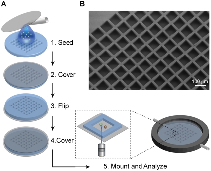
Figure 1
Preparation of PDMS chips for microscopy.
(A) Schematic drawing demonstrating chip preparation from seeding to microscopy. Cell suspension was added onto the primed chip (1), excess medium was removed, and the wells were sealed with a cover g...
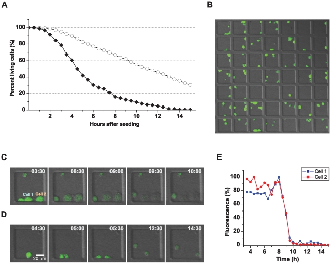
Figure 2
Cell survival in PDMS wells.
Calcein-AM-labeled 221 cells were seeded, confined in PDMS wells and imaged at 37u00b0C, 5% CO 2 . Images were acquired of 81 wells every 30 minutes for 15 hours. (A) Cell survival comparing two diffe...
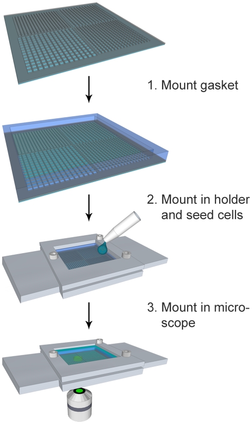
Figure 3
Preparation of silicon chips for microscopy.
The silicon chips were primed by degassing the chip submerged in cell medium until the wells were filled with medium. A PDMS-gasket was mounted onto the perimeter of the silicon chip (1). The chip was...
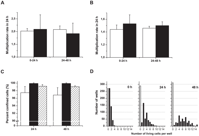
Figure 4
Cell survival and confinement in silicon wells.
(A, B) Multiplication rates in the wells (white bars) compared to conventional cell culturing in a tissue culture dish (black bars); 221 cells (A) and YTS cells (B). (C) Level of confinement was measu...
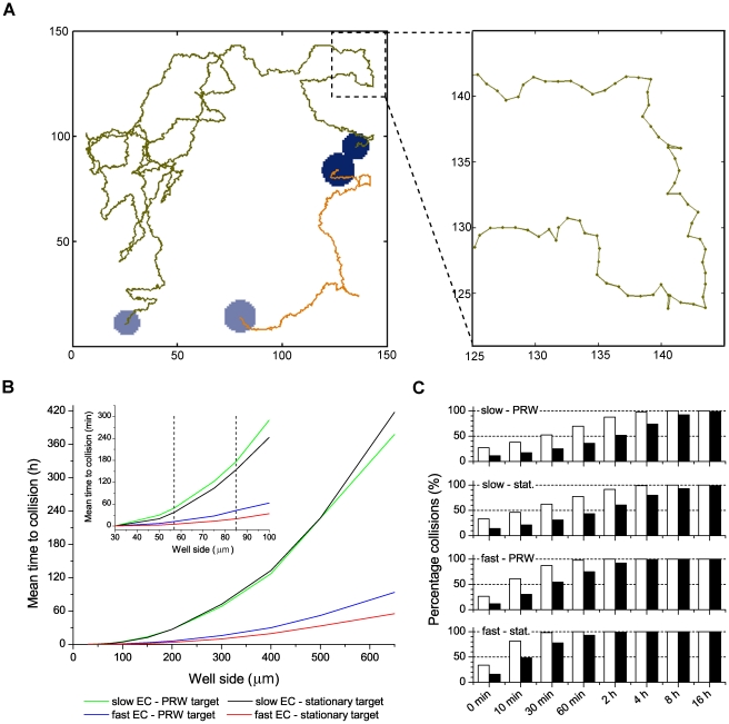
Figure 5
Simulation of time to cell-cell encounter in differently sized wells.
One target cell and one effector cell (EC) were randomly placed together in a square well and the mean time to collision was simulated running 1024 times for each well size. The EC was either migratin...
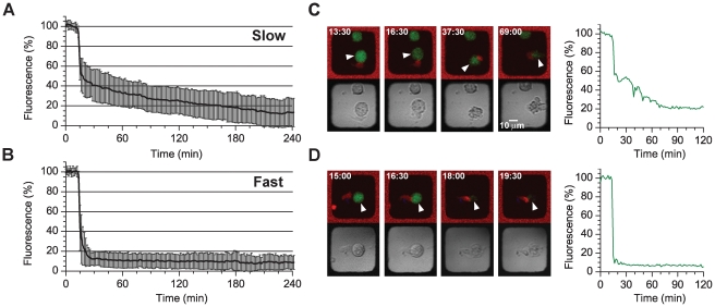
Figure 6
NK cell killing in microwells.
IL-2 activated primary human NK cells and 293T target cells were seeded together in a silicon microchip and imaged every 1.5 minutes for several hours. NK cells were stained with calcein red-orange (r...
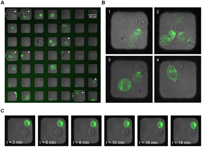
Figure 7
High-resolution imaging of immune synapse formation in microwells.
221/Cw6-GFP target cells (green) were seeded together with the unstained NK cell line YTS/KIR1, and the chip was imaged for synapse formation over time. Inhibitory immune synapse formation can be seen...
Figure images are served from the NIH/NLM PubMed Central Open Access Subset or Europe PMC; copyright remains with the publishers and authors.
💬 Discussion
0 commentsNo comments yet. Be the first to start a discussion!
Leave a Comment