Abstract
Abstract In the last couple of decades, the spatial resolution in optical microscopy has increased to unprecedented levels by exploiting the fluorescence properties of the probe. At about the same time, Raman imaging techniques have emerged as a way to image inherent chemical information in a sample without using fluorescent probes. However, in many applications, the achievable resolution is limited to about half the wavelength of excitation light. Here we report the use of structured illumination to increase the spatial resolution of label-free spontaneous Raman microscopy, generating highly detailed spatial contrast from the ensemble of molecular information in the sample. Using structured line illumination in slit-scanning Raman microscopy, we demonstrate a marked improvement in spatial resolution and show the applicability to a range of samples, including both biological and inorganic chemical component mapping. This technique is expected to contribute towards greater understanding of chemical component distributions in organic and inorganic materials.
🔬 Techniques
✨ Fluorophores
🧪 Sample Preparation
🏭 Microscope Brands
📷 Detectors
💾 Data Repositories
🏛️ Research Organizations (ROR)
Affiliated research institutions:
📋 Methods
SLI Raman imaging of carbon materials In Fig. 3 , we show how SLI Raman imaging provides enhanced spatial contrast for chemically distinct features in graphene. Graphene sheets and graphite fragments were observed and compared by the LI and SLI microscope. Nanocarbon-based materials, such as graphene, carbon nanotubes and graphite, are promising research targets owing to their exceptional performance in various applications ranging from the basic science to industrial applications 17 18 . As these carbon materials exhibit strong Raman scattering, Raman microscopy is often used to investigate the structural difference in carbon materials 19 . However, many of the features of interest are at scales below the diffraction limit of light, making them difficult to resolve with conventional Raman imaging. In Fig. 3a,b , the intensities of Raman peaks assigned to D (red), G (blue) and 2D (green) vibrational bands are used to visualize the small domain structures. These domains were confirmed as single-layer graphene, two-layer graphene, graphite and defect domains as shown in Fig. 3c . The comparison of Fig. 3a,b shows the unambiguous resolution improvement by SLI, where the reticulate pattern of defects is clearly visualized. The line profiles in Fig. 3d clearly show the improvement of the spatial resolution by SLI. The spectrum distribution shown in Fig. 3e reveals that the D band signal given by SLI has a strong correlation with the G band signal, but not with the 2D band. These correlations cannot be observed in the LI image, indicating the spectral overlap between neighbouring positions owing to the insufficient spatial resolution. We also observed a graphite fragment by the LI and SLI microscope as shown in Fig. 3f,g , respectively. The edge structure of the fragment and fine graphite surface features can be determined from the D and G band distributions only in the SLI imaging modality as shown in Fig. 3h .
Show full methods section
SLI Raman imaging of carbon materials In Fig. 3 , we show how SLI Raman imaging provides enhanced spatial contrast for chemically distinct features in graphene. Graphene sheets and graphite fragments were observed and compared by the LI and SLI microscope. Nanocarbon-based materials, such as graphene, carbon nanotubes and graphite, are promising research targets owing to their exceptional performance in various applications ranging from the basic science to industrial applications 17 18 . As these carbon materials exhibit strong Raman scattering, Raman microscopy is often used to investigate the structural difference in carbon materials 19 . However, many of the features of interest are at scales below the diffraction limit of light, making them difficult to resolve with conventional Raman imaging. In Fig. 3a,b , the intensities of Raman peaks assigned to D (red), G (blue) and 2D (green) vibrational bands are used to visualize the small domain structures. These domains were confirmed as single-layer graphene, two-layer graphene, graphite and defect domains as shown in Fig. 3c . The comparison of Fig. 3a,b shows the unambiguous resolution improvement by SLI, where the reticulate pattern of defects is clearly visualized. The line profiles in Fig. 3d clearly show the improvement of the spatial resolution by SLI. The spectrum distribution shown in Fig. 3e reveals that the D band signal given by SLI has a strong correlation with the G band signal, but not with the 2D band. These correlations cannot be observed in the LI image, indicating the spectral overlap between neighbouring positions owing to the insufficient spatial resolution. We also observed a graphite fragment by the LI and SLI microscope as shown in Fig. 3f,g , respectively. The edge structure of the fragment and fine graphite surface features can be determined from the D and G band distributions only in the SLI imaging modality as shown in Fig. 3h .
Methods
Experimental set-up A CW frequency-doubled Nd:YVO 4 laser (532 nm, Spectra-Physics, Millenia) was used as a light source for all the experiments. An imaging spectrophotometer (Bunko Keiki, MK-300) equipped with a cooled CCD camera (Princeton Instruments, PIXIS400B) was used for detecting Raman spectra. A total of 400 Raman spectra were measured simultaneously in one exposure. Two edge filters (Semrock, LPD01-532RU-25) were used to separate the laser and the Raman scattering light before the spectrophotometer. A commercial inverted microscope (Nikon, ECLIPSE Ti) was used for mounting the objective lens and sample, and a focus stabilization system (Nikon, Perfect Focus System) was used to keep the focal plane in the sample constant during the measurement. In all Raman imaging experiments, the slit width was set to the Airy size with the centre wavelength (591 nm) detected in the spectrophotometer, which corresponds to a spectral resolution of 3.1 cm −1 at the centre wavelength.
Image processing
First, we removed the cosmic rays detected in the measured spectra by using a median filter on the recorded CCD frame. The median filter was applied to a 5 × 5 pixels area centred on the pixel exhibiting a cosmic ray spike, which shows as a large spurious intensity far higher than the typical Raman intensity. The process was skipped if the cosmic ray did not exceed a threshold (typically six standard deviations above the local median). Cosmic ray spikes occur only at a few pixels in the CCD array, which means that the vast majority of the raw Raman data is unaffected by the median filtering process. The spectral data were then processed by subtraction of the CCD read-out background and pixel resampling for distortion compensation ( Supplementary Fig. 1 and Supplementary Note 1 ). For SLI images, we used the SIM reconstruction procedure described in ref. 9 . Briefly, we extract the spatial frequency components in the Fourier domain, and combine them appropriately with OTF compensation after moving the components back to their original positions in Fourier space. For OTF compensation, a Wiener filter is used with a parameter that is empirically determined as described in the SIM literature (see for example: refs 9 , 38 ) to minimize artifacts that arise during the image reconstruction process. The OTF of the imaging optics was determined from an image of a fluorescent bead with a diameter of 40 nm. In addition, a triangle window function is used to suppress edge-related artifacts. The reassembled image is then transferred to the real space domain. For LI images, we averaged three Raman images obtained with different fringe phases and resampled the resultant LI image by using spline interpolation to make the pixel number equal to that in the reconstructed SLI image. We applied singular value deposition (SVD) to the PS/PMMA image and the brain tissue image for noise reduction 39 . Briefly, SVD models the data into two sets of vectors weighted by singular values and by approximating the data matrix as a subset of singular values and vectors that contains primarily the relevant spectral features, the noise present in the data is reduced. Visual inspection of the rejected SVD vectors was performed to ensure that they contain predominantly noise and no strong spatial and spectral features. Savitzky–Golay fitting was applied to the graphene spectrum for smoothing. The fluorescence background was removed using a polynomial curve fitting technique 40 in the PS/PMMA beads and the brain tissue images.
Imaging of PS and PMMA mixture
PS and PMMA particles were dispersed in water and dropped onto a glass substrate (Matsunami, MAS-coated glass). An objective lens with an NA 1.27 WI, × 60 (Nikon, CFI Plan Apo IR × 60) was used for the observation. A phase grating of 92 grooves per millimetre (GPM), corresponding to a normalized offset distance of 0.48 (ref. 15 ), to produce the interference fringe on the line illumination, was used. The exposure time and excitation intensity were 5 s per line and 4.3 mW μm −2 , respectively. The pixel numbers of the image in the measurement were 200, 400 and 900 for x , y and λ directions, respectively. The scanning step size for the x direction was 143 nm. Graphene imaging A CVD graphene sheet was purchased from Graphene Platform and placed on the microscope stage for observation. An NA 0.95 dry objective lens (Nikon, CFI Plan Apo λ × 60) was used for the observation. A phase grating of 80 GPM, corresponding to a normalized offset distance of 0.56 (ref. 15 ), to produce the interference fringes in the line illumination, was used. The exposure time and the excitation intensity were 10 s per line and 2 mW μm −2 , respectively. The pixel numbers of the image in the measurement were 200, 400 and 900 for x , y and λ directions, respectively. The scanning step size for the x direction was 143 nm.
Graphite imaging
Thin layered graphite was prepared through mechanical cleavage of highly ordered pyrolytic graphite (HOPG; SPI supplies, 476HP-AB). The same objective lens and the phase grating pair used in the PS/PMMA imaging were applied. The exposure time and the excitation intensity were 5 s per line and 0.85 mW μm −2 , respectively. The pixel numbers of the image in the measurement were 50, 400 and 900 for x , y and λ directions, respectively. The scanning step size for x direction was 109 nm.
Mouse brain tissue imaging
Animal experiments were performed in accordance with the guidelines of the Japanese Pharmacological Society, and were approved by the Animal Care and Use Committee of the Graduate School of Pharmaceutical Sciences, Osaka University. All efforts were made to minimize the number of animals used. Adult male C57BL/6 mice were anaesthetized with sodium pentobarbital (50 mg kg −1 , intraperitoneally), and perfused through the left ventricle with 4% paraformaldehyde in phosphate-buffered saline (4% PFA). Brains were removed, fixed overnight at 4 °C in 4% PFA and sliced at a thickness of 20 μm in phosphate-buffered saline on a Leica vibratome (VT 1000S). The same objective lens and phase grating pair used in the PS/PMMA imaging were applied. The exposure time and the excitation intensity were 10 s per line and 4.3 mW μm −2 , respectively. The pixel numbers of the image in the measurement were 200, 400 and 900 for x, y and λ directions, respectively. The scanning step size for the x direction was 143 nm.
Experimental set-up A CW frequency-doubled Nd:YVO 4 laser (532 nm, Spectra-Physics, Millenia) was used as a light source for all the experiments. An imaging spectrophotometer (Bunko Keiki, MK-300) equipped with a cooled CCD camera (Princeton Instruments, PIXIS400B) was used for detecting Raman spectra. A total of 400 Raman spectra were measured simultaneously in one exposure. Two edge filters (Semrock, LPD01-532RU-25) were used to separate the laser and the Raman scattering light before the spectrophotometer. A commercial inverted microscope (Nikon, ECLIPSE Ti) was used for mounting the objective lens and sample, and a focus stabilization system (Nikon, Perfect Focus System) was used to keep the focal plane in the sample constant during the measurement. In all Raman imaging experiments, the slit width was set to the Airy size with the centre wavelength (591 nm) detected in the spectrophotometer, which corresponds to a spectral resolution of 3.1 cm −1 at the centre wavelength.
Supplementary Material Supplementary Information Supplementary Figures 1-2 and Supplementary Notes 1-2
📊 Figures
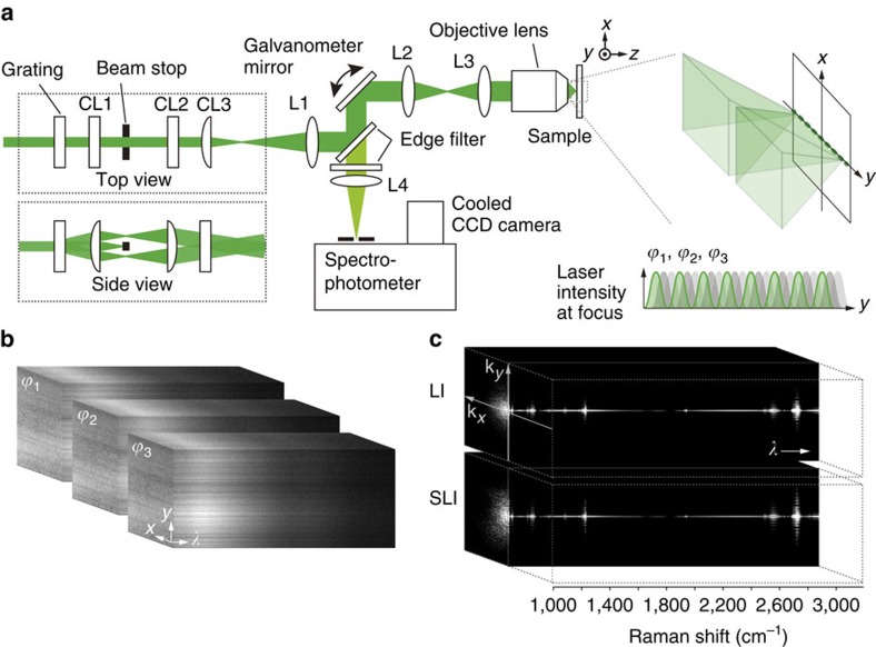
Figure 1
SLI Raman microscopy.
( a ) A schematic optical system of SLI Raman microscopy. CL and L represent a cylindrical lens and lens, respectively. ( b ) Hyperspectral images of a fluorescent PMMA film of Rhodamine 6G obtained w...
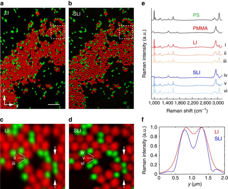
Figure 2
Raman images of polystyrene (green) and poly(methyl methacrylate) (red) beads.
( a , b ) LI ( a ) and SLI ( b ) images from the same position in the sample constructed by the Raman signal at 3,055u2009cm u22121 (polystyrene, PS) and 2,957u2009cm u22121 (poly(methyl methacrylate)...
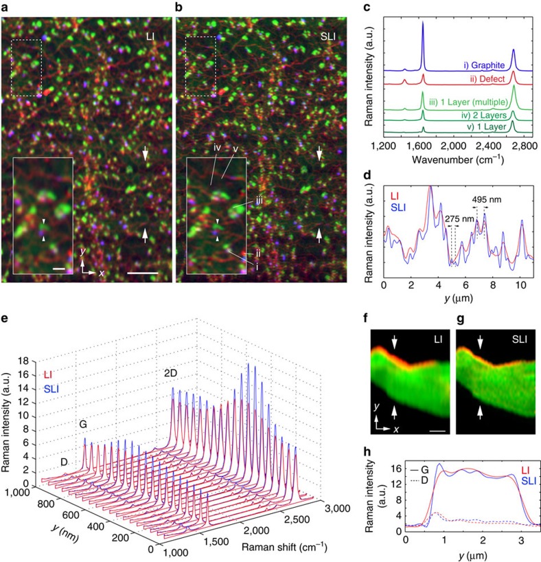
Figure 3
Raman images of carbon materials.
( a , b ) LI ( a ) and SLI ( b ) Raman images of a graphene sheet grown by chemical vapour deposition. The images were constructed with the distributions of D (1,307u20131,387u2009cm u22121 averaged, ...
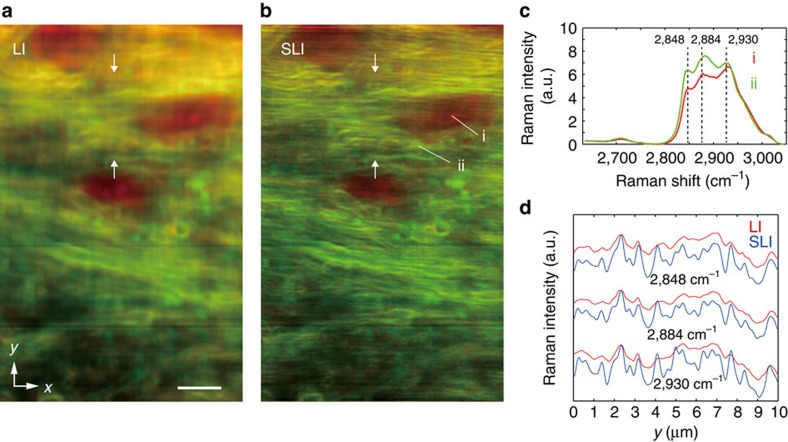
Figure 4
Raman images of a mouse brain slice.
( a , b ) The intensity distribution of Raman peaks at 1,682u2009cm u22121 (red) and 2,848u2009cm u22121 (green) imaged by the LI ( a ) and SLI ( b ) microscopes (Scale bar, 5u2009u03bcm). Raman peaks...
Figure images are served from the NIH/NLM PubMed Central Open Access Subset or Europe PMC; copyright remains with the publishers and authors.
💬 Discussion
0 commentsNo comments yet. Be the first to start a discussion!
Leave a Comment