Abstract
In neural interface platforms, cultures are often carried out on a flat, open, rigid, and opaque substrate, posing challenges to reflecting the native microenvironment of the brain and precise engagement with neurons. Here we present a neuron cell culturing platform that consists of arrays of ordered microtubes (2.7-4.4 μm in diameter), formed by strain-induced self-rolled-up nanomembrane (s-RUM) technology using ultrathin (<40 nm) silicon nitride (SiNx) film on transparent substrates. These microtubes demonstrated robust physical confinement and unprecedented guidance effect toward outgrowth of primary cortical neurons, with a coaxially confined configuration resembling that of myelin sheaths. The dynamic neural growth inside the microtube, evaluated with continuous live-cell imaging, showed a marked increase (20×) of the growth rate inside the microtube compared to regions outside the microtubes. We attribute the dramatic accelerating effect and precise guiding of the microtube array to three-dimensional (3D) adhesion and electrostatic interaction with the SiNx microtubes, respectively. This work has clear implications toward building intelligent synthetic neural circuits by arranging the size, site, and patterns of the microtube array, for potential treatment of neurological disorders.
🔬 Techniques
🧪 Sample Preparation
🔬 Cell Lines
🏭 Microscope Brands
🧪 Reagent Suppliers
🏛️ Research Organizations (ROR)
Affiliated research institutions:
📋 Methods
SiNx Bilayer Deposition, Microtube Fabrication, and Morphology/Topology Tuning For the thin membrane to roll, sufficient strain must be embedded in the film, placing a constraint on the system. Compressive strain must be embedded in at least a fraction of one component to provide an expanding force, followed by one of two actions. The method used in this study relies primarily on changing the plasma frequency. 42 Alternatively, one can begin the plasma deposition at a higher temperature, reducing temperature as deposition proceeds. 32 As seen in Figures 1 and 2 , two methods are employed to achieve microtube arrays ( Figure 4 ), depending on etchant speed and uniformity: timed etching (process #1) and anchored membranes (process #2), for slow and fast etches, respectively. This study focuses on the former to achieve single and binocular shaped microtubes on silicon substrates. The latter is employed during live-cell imaging to achieve single roll microtubes secured with a robust anchor to No. 1.5 coverslips. Figure 4 Fabrication process for a rolled up SiNx microtube: (a) deposition of sacrificial layer and compressively strained LF layer, followed by deposition of tensile strained HF-layer; (b) formation of rectangular mesa (optional) deposition of 100 nm PECVD SiO x anchor, and either released from (c) both sides (process #1) or (d) one side (process #2). In both processes, the initial pad dimensions determine the final geometry. (f) Microtube diameter is determined by both LF and HF layer thickness. The deriving mathematics was previously described. 42 Deposition and fabrication of SiN x -based microtubes can be condensed to three crucial steps ( Figure 4 a–d): deposition of sacrificial layer and strained SiN x bilayer, patterning and dry etch, and sacrificial layer etching, which releases built in strain and causes rolling from all unanchored sides. Strain, and thus diameter, in SiN x microtubes is influenced by PECVD deposition parameters and postfabrication thermal processing. 42 Specifically, the sacrificial layer used here was either a (111) silicon substrate or germanium on a SiO 2 substrate. When fabricating biologically compatible rolled-up interfaces, it is intuitive that additional care must be taken to remove residual contamination before beginning a culture. Initially, Si (111) substrates were utilized as sacrificial layers due to a low vertical etch rate and low film porosity, achieving the most uniform arrays on silicon. Under SEM inspection ( Figure 1 c), sparse residue was identified on the substrate between microtubes. As an improvement over KOH etching, a germanium sacrificial layer was employed and successively etched in H 2 O 2 , which simultaneously cleaned the sample. In both cases the sacrificial layer is sonicated in acetone to remove any organic contamination and then subjected to a native oxide etch. If germanium is to be used, e-beam evaporated Ge is deposited at a rate of 1 nm/sec under 1–2 μTorr to a thickness of 20–80 nm. The strained bilayer consists of a 15–20 nm low frequency PECVD SiN x (under compressive strain) capped by a 15–20 nm high frequency SiN x (tensile). The mesa is patterned with AZ5214E and CF 4 is used to dry etch through the bilayer and into sacrificial layer. The photoresist is removed and the sacrificial layer is etched with 30% H 2 O 2 at 80 °C for Ge and 45% KOH at 80C for Si. 42 Finally, the layers are immersed in methanol for 5 min and dried on hot plate at 80 °C. To achieve binocular shaped microtubes ( Figure 1 c) instead of single rolled microtubes, the initial mesa width must be equal to or larger than twice the final circumference. Per fabrication process #1 ( Figure 4 c), the sacrificial layer is removed from everywhere on the sample except a small anchor (∼500 nm) under the microtube, exposing the underlying substrate and resulting in an elevated microtube (∼20 nm). In contrast, process #2 ( Figure 4 d) results in microtubes anchored to the substrate and rolled from one side, removing the effect of this gap.
Show full methods section
SiNx Bilayer Deposition, Microtube Fabrication, and Morphology/Topology Tuning For the thin membrane to roll, sufficient strain must be embedded in the film, placing a constraint on the system. Compressive strain must be embedded in at least a fraction of one component to provide an expanding force, followed by one of two actions. The method used in this study relies primarily on changing the plasma frequency. 42 Alternatively, one can begin the plasma deposition at a higher temperature, reducing temperature as deposition proceeds. 32 As seen in Figures 1 and 2 , two methods are employed to achieve microtube arrays ( Figure 4 ), depending on etchant speed and uniformity: timed etching (process #1) and anchored membranes (process #2), for slow and fast etches, respectively. This study focuses on the former to achieve single and binocular shaped microtubes on silicon substrates. The latter is employed during live-cell imaging to achieve single roll microtubes secured with a robust anchor to No. 1.5 coverslips. Figure 4 Fabrication process for a rolled up SiNx microtube: (a) deposition of sacrificial layer and compressively strained LF layer, followed by deposition of tensile strained HF-layer; (b) formation of rectangular mesa (optional) deposition of 100 nm PECVD SiO x anchor, and either released from (c) both sides (process #1) or (d) one side (process #2). In both processes, the initial pad dimensions determine the final geometry. (f) Microtube diameter is determined by both LF and HF layer thickness. The deriving mathematics was previously described. 42 Deposition and fabrication of SiN x -based microtubes can be condensed to three crucial steps ( Figure 4 a–d): deposition of sacrificial layer and strained SiN x bilayer, patterning and dry etch, and sacrificial layer etching, which releases built in strain and causes rolling from all unanchored sides. Strain, and thus diameter, in SiN x microtubes is influenced by PECVD deposition parameters and postfabrication thermal processing. 42 Specifically, the sacrificial layer used here was either a (111) silicon substrate or germanium on a SiO 2 substrate. When fabricating biologically compatible rolled-up interfaces, it is intuitive that additional care must be taken to remove residual contamination before beginning a culture. Initially, Si (111) substrates were utilized as sacrificial layers due to a low vertical etch rate and low film porosity, achieving the most uniform arrays on silicon. Under SEM inspection ( Figure 1 c), sparse residue was identified on the substrate between microtubes. As an improvement over KOH etching, a germanium sacrificial layer was employed and successively etched in H 2 O 2 , which simultaneously cleaned the sample. In both cases the sacrificial layer is sonicated in acetone to remove any organic contamination and then subjected to a native oxide etch. If germanium is to be used, e-beam evaporated Ge is deposited at a rate of 1 nm/sec under 1–2 μTorr to a thickness of 20–80 nm. The strained bilayer consists of a 15–20 nm low frequency PECVD SiN x (under compressive strain) capped by a 15–20 nm high frequency SiN x (tensile). The mesa is patterned with AZ5214E and CF 4 is used to dry etch through the bilayer and into sacrificial layer. The photoresist is removed and the sacrificial layer is etched with 30% H 2 O 2 at 80 °C for Ge and 45% KOH at 80C for Si. 42 Finally, the layers are immersed in methanol for 5 min and dried on hot plate at 80 °C. To achieve binocular shaped microtubes ( Figure 1 c) instead of single rolled microtubes, the initial mesa width must be equal to or larger than twice the final circumference. Per fabrication process #1 ( Figure 4 c), the sacrificial layer is removed from everywhere on the sample except a small anchor (∼500 nm) under the microtube, exposing the underlying substrate and resulting in an elevated microtube (∼20 nm). In contrast, process #2 ( Figure 4 d) results in microtubes anchored to the substrate and rolled from one side, removing the effect of this gap.
Preculture Microtube Preparation
The microtube-contained substrate was stored in 70% ethyl alcohol for cleaning and sterilizing. Prior to poly- d -lysine (PDL) coating, the sterilized substrate was carefully flooded by preautoclaved milli-Q deionized water three times to rinse off the alcohol. Beginning at this point, every following procedure was performed in a sterile environment. The substrate was subsequently dried and treated with UV exposure for 15 min, followed by PDL coating. Poly- d -lysine in a final concentration of 0.1 mg/mL was used to coat the substrate surface and facilitate cell adhesion. Cortical Neural Culturing For the axon guidance study, E15.5 cortical neurons obtained from Swiss Webster mice were used. Briefly, the cells were dissociated by treating with trypsin (0.25%, 15 min, 37 °C), then triturated, diluted in plating medium (neurobasal medium with 5% FBS, Hyclone, B27 supplement, 2 mMglutamine, 37.5 mMNaCl, and 0.3% glucose), and plated onto the substrates in a 35 mm Petri dish. Cells were seeded at either low density (5000 cells/cm 2 ) or high density (50 000 cells/cm 2 ) as indicated in the Results section. After 1 h, the sample was flooded with serum-free medium (plating medium without FBS) and cultured for 5–7 days, or as indicated elsewhere.
Immunostaining and Fluorescent Imaging
The culture sample for fluorescent imaging was fixed in 4% paraformaldehyde/Krebs/sucrose at pH 7.4, blocked with 10% BSA/PBS, permeabilized in 0.2% Trition X-100/PBS, and labeled with antibodies to tyrosinated tubulin at 1:1000 (YL1/2 clone, Chemicon 64 ). Secondary antibodies coupled to Alexa 568 (Invitrogen) were used at 1:500. The immunostained cell cultures were imaged with a Fluoview500 AX70 upright (Olympus, USA) microscope through a 40× water-immersion lens of numerical aperture 0.8.
Sample Preparation and SEM Imaging
Prior to SEM imaging, the cell culture was fixed in mixed primary fixative of 2% paraformaldehyde/Krebs/sucrose and 2.5% glutaraldehyde in phosphate buffer at pH 7.4 for 30 min, then rinsed three times with phosphate buffered saline (PBS) solution. The cell culture was then treated with a postfixative of 1% osmium tetraoxide in phosphate buffer at pH 7.4 for 1 h, and then rinsed thoroughly with PBS solution. The fixed sample was dehydrated through an ethanol series with 10%–90%, and three times 100%, over 30 min. The dehydrated sample was then dried in a critical point dryer, and sputter-coated with ∼2 nm gold–palladium. SEM images were taken with a LEO Gemini 1530 at 45° tilting.
Live Cell Imaging
The neural culture after 2–5 DIV was imaged using a BioStation integrated microscope (Nikon, Inc.) through a 20× lens. A phase contrast image was captured every 15 min for 18–48 h. Details of equipment setup was previously described. 6
Supplementary Material nn504876y_si_001.avi nn504876y_si_002.avi nn504876y_si_003.pdf
📊 Figures
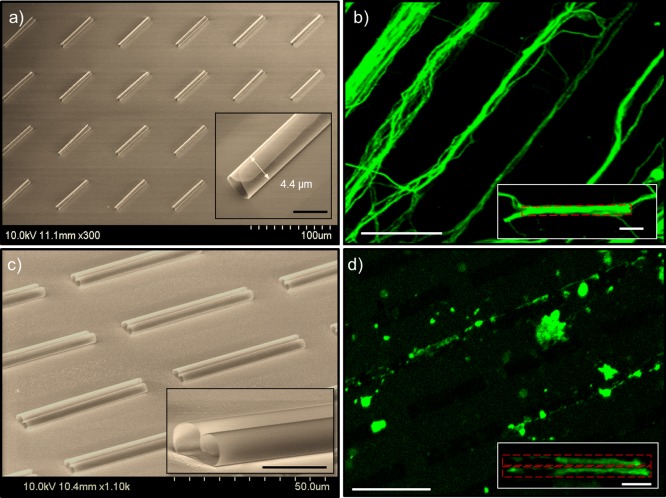
Figure 1
SEM images (a and c) of SiNx microtube array and the corresponding immunocytochemistry of neural culture fluorescence images (b and d). (a) Single roll and (c) binocular-shaped double roll SiNx microt...
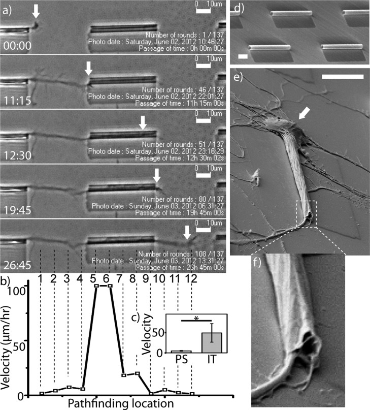
Figure 2
Outgrowth of a single neuron in a microtube. (a) Time-lapse phase contrast images of a living cortical neuron show axonal pathfinding through a microtube. Each frame, from top to bottom, represents gr...
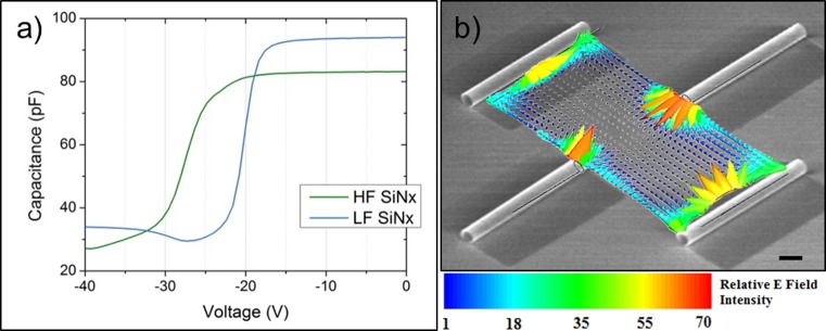
Figure 3
Electrostatic effect of SiN x microtubes. (a) High frequency capacitanceu2013voltage ( C u2013 V ) measurement of tensile HF- and compressive LF-SiN x reveals a large flat band voltage shift to the le...
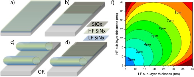
Figure 4
Fabrication process for a rolled up SiNx microtube: (a) deposition of sacrificial layer and compressively strained LF layer, followed by deposition of tensile strained HF-layer; (b) formation of recta...
Figure images are served from the NIH/NLM PubMed Central Open Access Subset or Europe PMC; copyright remains with the publishers and authors.
💬 Discussion
0 commentsNo comments yet. Be the first to start a discussion!
Leave a Comment