Abstract
Using high resolution focused ion beam scanning electron microscopy (FIB-SEM) we study the details of cell-nanostructure interactions using serial block face imaging. 3T3 Fibroblast cellular monolayers are cultured on flat glass as a control surface and on two types of nanostructured scaffold substrates made from silicon black (Nanograss) with low- and high nanowire density. After culturing for 72 hours the cells were fixed, heavy metal stained, embedded in resin, and processed with FIB-SEM block face imaging without removing the substrate. The sample preparation procedure, image acquisition and image post-processing were specifically optimised for cellular monolayers cultured on nanostructured substrates. Cells display a wide range of interactions with the nanostructures depending on the surface morphology, but also greatly varying from one cell to another on the same substrate, illustrating a wide phenotypic variability. Depending on the substrate and cell, we observe that cells could for instance: break the nanowires and engulf them, flatten the nanowires or simply reside on top of them. Given the complexity of interactions, we have categorised our observations and created an overview map. The results demonstrate that detailed nanoscale resolution images are required to begin understanding the wide variety of individual cells' interactions with a structured substrate. The map will provide a framework for light microscopy studies of such interactions indicating what modes of interactions must be considered.
🔬 Techniques
🧪 Sample Preparation
🔬 Cell Lines
🏭 Microscope Brands
🧪 Reagent Suppliers
💻 Software Details
🏛️ Research Organizations (ROR)
Affiliated research institutions:
📋 Methods
Nanostructure Substrate Fabrication Two different black silicon substrates also known as “nanograss” [41] were used: one provides high density silicon nanograss (Nanograss A), while the other has sparser nanowires (Nanograss B). A table of the substrates’ different characteristics can be seen in Table 1 , refer to Figure S1 for SEM images of the substrates. 10.1371/journal.pone.0053307.t001 Table 1 Overview of the different nanostructured substrates, their processing parameters, and their morphology. Sample Height [nm] Width [nm] Density [1/µm2] Nanograss A 990±190 80±60 9.6±0.8 Nanograss B 1170±280 70±40 4.5±0.3 The uncertainties are 2 times the standard deviation giving a two sigma/95% confidence. The black silicon nanograss was made from 4″ low doped silicon wafers using maskless deep reactive ion etching (DRIE). Differing nanostructures were obtained by controlling the reactive ion etch parameters [42] . For instance the density is controlled by varying the process chamber pressure and coil electrode power, whereas the height scales linearly with processing time. DRIE was performed in an advanced silicon etcher (Surface Technology Systems), the SF 6 /O 2 ratio was 1.11, while the platen power was 120 W, and the chamber pressure was between 8 and 56 mTorr. This formed nanostructured “silicon grass” at a rate of about 2 nm/s [42] .
Cell Monolayer Culturing Mouse embryonic fibroblasts
(NIH3T3) were cultured on plain glass substrates, and 10×10 mm diced silicon chips with Nanograss A and Nanograss B ( Table 1 ). Before culturing, the chips were sterilised with 70% ethanol for 20 minutes, and flushed 3–4 times with pure water or PBS. The cells were cultured in Dulbecco’s modified Eagle’s medium with Glutamax (DMEM; GIBCO Life Technologies), 10% fetal bovine serum (FBS; Sigma) and 1% penicillin-streptomycin (P/S; GIBCO Life Technologies). Standard conditions of 37°C and an atmosphere of 5% CO 2 were applied. As capillary forces during drying is known to incur nanowire bending and clustering [43] , care was taken to always have liquid covering the samples during preparation.
Show full methods section
Nanostructure Substrate Fabrication Two different black silicon substrates also known as “nanograss” [41] were used: one provides high density silicon nanograss (Nanograss A), while the other has sparser nanowires (Nanograss B). A table of the substrates’ different characteristics can be seen in Table 1 , refer to Figure S1 for SEM images of the substrates. 10.1371/journal.pone.0053307.t001 Table 1 Overview of the different nanostructured substrates, their processing parameters, and their morphology. Sample Height [nm] Width [nm] Density [1/µm2] Nanograss A 990±190 80±60 9.6±0.8 Nanograss B 1170±280 70±40 4.5±0.3 The uncertainties are 2 times the standard deviation giving a two sigma/95% confidence. The black silicon nanograss was made from 4″ low doped silicon wafers using maskless deep reactive ion etching (DRIE). Differing nanostructures were obtained by controlling the reactive ion etch parameters [42] . For instance the density is controlled by varying the process chamber pressure and coil electrode power, whereas the height scales linearly with processing time. DRIE was performed in an advanced silicon etcher (Surface Technology Systems), the SF 6 /O 2 ratio was 1.11, while the platen power was 120 W, and the chamber pressure was between 8 and 56 mTorr. This formed nanostructured “silicon grass” at a rate of about 2 nm/s [42] .
Cell Monolayer Culturing Mouse embryonic fibroblasts
(NIH3T3) were cultured on plain glass substrates, and 10×10 mm diced silicon chips with Nanograss A and Nanograss B ( Table 1 ). Before culturing, the chips were sterilised with 70% ethanol for 20 minutes, and flushed 3–4 times with pure water or PBS. The cells were cultured in Dulbecco’s modified Eagle’s medium with Glutamax (DMEM; GIBCO Life Technologies), 10% fetal bovine serum (FBS; Sigma) and 1% penicillin-streptomycin (P/S; GIBCO Life Technologies). Standard conditions of 37°C and an atmosphere of 5% CO 2 were applied. As capillary forces during drying is known to incur nanowire bending and clustering [43] , care was taken to always have liquid covering the samples during preparation.
Cell Monolayer Post-culture Processing
After culturing for 72 hours the cells were fixed, stained and embedded (cf. Text S1 for the full protocol). First, the samples were fixed with 2% glutaraldehyde in 0.05 M sodium cacodylate buffer, pH 7.2 (isotonic, 300 mOsm) for 1 hr, rinsed in 0.15 M sodium cacodylate buffer pH 7.2 (2×30 min), and postfixed in 1% osmium tetroxide in 0.12 M cacodylate buffer pH 7.2 (isotonic, 300 mOsm) for 1 hour. Next, the specimens were rinsed in Milli-Q water (2×10 min) to remove osmium residues, and stained with 1% tannic acid in Milli-Q for 1 hr. Following a rinse in Milli-Q (2×10 min), the sample was stained with 1% uranyl acetate for 2 hrs. The specimens were dehydrated and embedded in Epon according to standard procedures, please refer to Text S1 for the full protocol. The polymerised Epon formed a meniscus over the substrate, leading to a thick resin layer in the centre and a thinner layer near the chip edges. This meant that a circular band of cells were directly accessible with the FIB-SEM, with an excessive thick layer in the centre which thinned out towards the periphery leaving only collapsed cells outermost. FIB-SEM Two FIB-SEM beam systems from FEI were used: the Quanta FEG 3D, and the Helios NanoLab600. The first system makes use of a dedicated backscatter detector and the second an in-lens detector. The cells of interest were localised from atop in standard SEM, using the highest acceleration voltage (30 kV) to detect cells underneath the embedding material (cf. Figure S2 ). In this paper, results are presented which were typically buried 5 µm deep in the embedding medium (cell top to surface). When a cell of interest was located, the acceleration voltage was lowered to 1.5–5 kV depending on the equipment and crossover alignment of both electron and ion beams was performed. To gain access to the cell, rough milling at high ion beam current was used, forming a trench in front of the cell. The time for trench milling was approximately 10–20 minutes, followed by finer milling prior to image recording. Both microscopes have installed G2 Slice and View software provided by FEI Company. It offers recording of slice stacks with a practical slice thickness as low as 10 nm in our experience, and image sizes and resolution allowing detailed imaging of whole cells. The thickness is limited by the ion beam alignment and stability and not the software. Automatic refocusing of the image is possible when the specimen holder is tilted and milling is done normal to the sample surface, but not for larger samples where non-tilted milling had to be performed (also called slanted milling [40] ). To avoid damaging the dedicated vC backscatter detector in the Quanta FEG 3D large samples could not be tilted. Thus to compare non-tilted and tilted sample images a post-processing algorithm was developed to get representative image volumes and comparable images (please refer to Text S2 ). Besides allowing milling of large samples, another advantage of non-tilted milling is the decreased brightness gradient resulting from deep trench imaging [40] . However, this process is more computational heavy, and suffers more if the slice thickness is not sufficient for resolving 1D nanostructures compared to tilted-milling. If the slice thickness is not sufficiently small for resolving the 1D nanostructures, slanted milling (horizontal sample) would to a larger degree lead to these appearing as pearls on a string (see images of cells on Nanograss B).
Image Processing
After the slice and view stack has been recorded several steps are required to convert it into a useful 3D dataset. To do this three steps are required: image scaling to correct for imaging on a slanted surface; alignment of the individual slices; and a coordinate transformation to match the original volume – all of which was done with the open source ImageJ software. The image is first scaled to obtain the image aspect ratio of the true slice surface instead of the compressed projection image from the tilted view. When image stacks are obtained, small random shifts between the slices occur, which is corrected with the stackreg plugin for imageJ. Lastly, affine volume transformations and rotation is performed to level the substrate to reshape the image volume to the original sample geometry. This procedure was done both for ordinary tilted milling, but also for non-tilted milling showing how a representative 3D stack can be obtained also when using non-tilted milling. To illustrate some of these transformations, the image stack obtained with non-tilted milling of a cell on glass can be observed from the side in Figure 1 . For further detail refer to . 10.1371/journal.pone.0053307.g001 Figure 1 Side views of the non-tilted milling obtained image stack of a cell on glass showing the sequential processing operations’ effects. A) The individual slices have been aligned forming a fairly smooth image using stack-reg algorithm. B) Then the substrate is corrected such as to annul the effects of automatic E-beam shifts in the Slice and View program, resulting in a 52 degree substrate. C) Finally the image stack is rotated 52 degrees to represent the sample on the flat substrate having been cut at an angle.
Supporting Information Figure S1 SEM images of the two types of nanograss substrates used. The two upper images show ordinary SEM images of the substrates, whereas the two below show the nanograss substrates having endured the embedding process. The embedded substrate images show standing nanowires and some which have tilted like the non embedded ones. (TIF) Click here for additional data file. Figure S2 Examples of SEM images taken from above at 30 kV, showing cells lying on a nanostructured substrate underneath an embedding layer. Left, image of cells (lighter grey) that can be found from atop on a good sample obtained with backscatter detector. The small white dots are small defects in the surface of the embedding layer. Right, secondary electron signal also shows visible cells underneath the epon, but with less contrast. (TIF) Click here for additional data file. Figure S3 Overview image where the EM images have been inverted. (TIF) Click here for additional data file. Figure S4 Illustrating the hollow circular and cylindrical cross sections observed depending on the angle of milling and the orientation of the nanowire. Notice how the nanowires appear to be hollow, whereas they are expected to be solid. (TIF) Click here for additional data file. Figure S5 Nanograss A showing standing nanowires next to the cell. (TIF) Click here for additional data file. Figure S6 Images illustrating the variance also observable for Nanograss B. To the left internalised nanowires are shown, and to the right a cell resting on top of nanowires can be viewed. (TIF) Click here for additional data file. Text S1 Supplementary information describing the embedding protocol used for embedding cells on substrates. (DOCX) Click here for additional data file. Text S2 Here the image processing after the slice and view process is explained. The developed steps for data processing of an image stack obtained both on a tilted and non-tilted substrate is described. (DOCX) Click here for additional data file.
📊 Figures
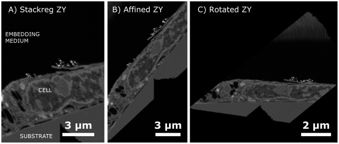
Figure 1
Side views of the non-tilted milling obtained image stack of a cell on glass showing the sequential processing operationsu2019 effects.
A) The individual slices have been aligned forming a fairly smooth image using stack-reg algorithm. B) Then the substrate is corrected such as to annul the effects of automatic E-beam shifts in the Sl...
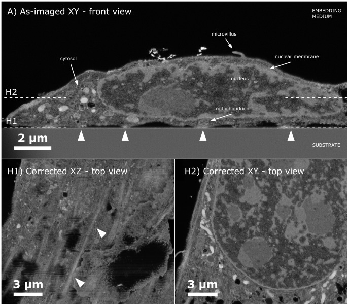
Figure 2
FIB-SEM image of cell on glass showing front view and top views. A)
Front view shows a non-processed as-imaged slice of a cell on a glass substrate. One can see the nucleus, microvillius, and organelles such as mitochondria in the cell cytosol. The triangular arrows h...
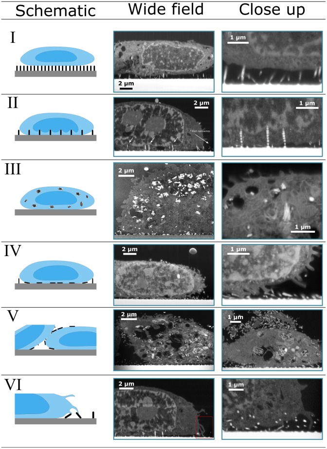
Figure 3
Map of the various cell-nanowire interactions observed.
6 cases are outlined with a schematic view and two supporting FIB-SEM images illustrating the case. Case VII, vacuolisation is to a large degree observed in images displaying Case III and Case VI.Inve...
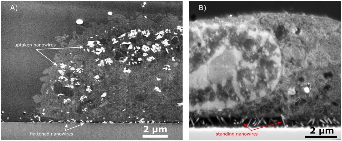
Figure 4
FIB-SEM image of cells on Nanograss A, illustrating different cell behaviours on the same substrate. A)
FIB-SEM image showing a cell having engulfed broken-off nanowires, and clearly bent silicon nanowires underneath the cell. The nanowires are closely packed in tightly formed clusters inside what appea...
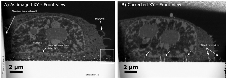
Figure 5
FIB-SEM images of a cell on Nanograss B. A)
As imaged (y-corrected) slice showing the nanowires which appear as white dots due to insufficient sampling frequency. Also worth noting is the example of Case III behaviour with microvili probing the...
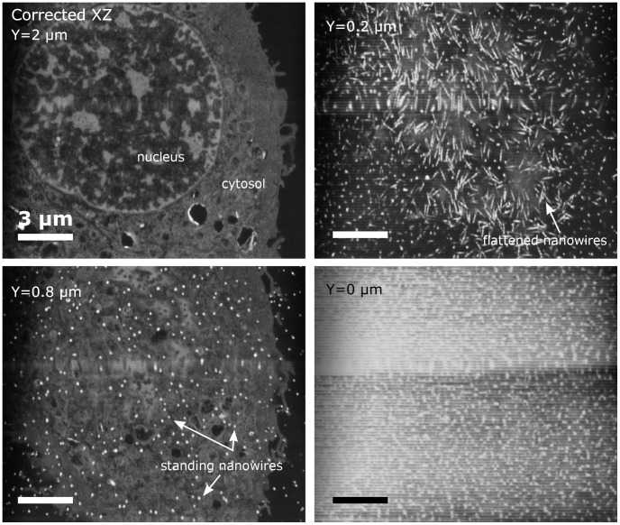
Figure 6
Image series showing the top view FIB-SEM image of the same cell as in Figure 5 on Nanograss B.
The sections have been made from 5 u00b5m above the substrate to 0.25 u00b5m above the substrate. This illustrates the major forces in play, clearly showing how several nanowires where bent underneath...
Figure images are served from the NIH/NLM PubMed Central Open Access Subset or Europe PMC; copyright remains with the publishers and authors.
💬 Discussion
0 commentsNo comments yet. Be the first to start a discussion!
Leave a Comment