Abstract
AbstractAtomic dopants and defects play a crucial role in creating new functionalities in 2D transition metal dichalcogenides (2D TMDs). Therefore, atomic‐scale identification and their quantification warrant precise engineering that widens their application to many fields, ranging from development of optoelectronic devices to magnetic semiconductors. Scanning transmission electron microscopy with a sub‐Å probe has provided a facile way to observe local dopants and defects in 2D TMDs. However, manual data analytics of experimental images is a time‐consuming task, and often requires subjective decisions to interpret observed signals. Therefore, an approach is required to automate the detection and classification of dopants and defects. In this study, based on a deep learning algorithm, fully convolutional neural network that shows a superior ability of image segmentation, an efficient and automated method for reliable quantification of dopants and defects in TMDs is proposed with single‐atom precision. The approach demonstrates that atomic dopants and defects are precisely mapped with a detection limit of ≈1 × 1012 cm−2, and with a measurement accuracy of ≈98% for most atomic sites. Furthermore, this methodology is applicable to large volume of image data to extract atomic site‐specific information, thus providing insights into the formation mechanisms of various defects under stimuli.
🔬 Techniques
🧪 Sample Preparation
💻 Software Details
🏛️ Research Organizations (ROR)
Affiliated research institutions:
📋 Methods
4.1 4.1.1 Synthesis of Pristine and V‐Doped TMD Monolayers Pristine and V‐doped WSe 2 (or MoS 2 ) samples were grown using an atmospheric CVD system. The liquid precursor for the growth of WSe 2 (or MoS 2 ) was prepared by mixing ammonium metatungstate, (or ammonium molybdate) and NaOH promoter. Additionally, ammonium metavanadate was introduced into the liquid precursor for V‐doping. The details of which are presented in Ref. [ 4 ]. The prepared liquid precursor was subsequently spin‐casted onto a SiO 2 /Si substrate, followed by selenization (or sulfurization) in the CVD chamber. To separately control the evaporation of selenium (or sulfur) and the reaction temperature, a two‐zone furnace CVD was adopted. For the growth of WSe 2 (or MoS 2 ), the Se (or S) was heated up to 400 °C at a rate of 50 °C min −1 (or 25 °C min −1 ), while the temperature of the substrate zone was elevated to 760 or 850 °C. Nitrogen and hydrogen gases at flow rates of 500 and 5 sccm, respectively, were injected during the CVD process. After the growth of the TMD, the furnace was naturally cooled to room temperature. DFT Calculations Spin‐polarized DFT calculations were conducted using the Vienna ab initio simulation package. [ 32 ] Here, the revised Perdew−Burke−Ernzerhof type exchange and correlation functional was employed. [ 33 ] The projector augmented wave (PAW) method was used for ion interaction. The Brillouin zone was sampled using a Г‐centered 3 × 3 × 1 k‐point mesh, while the electronic states were smeared using the Methfessel−Paxton scheme with a broadening width of 0.1 eV. The electronic wave functions were expanded in a plane wave basis with a cutoff energy of 400 eV and the atomic relaxation was continued until the Hellmann−Feynman forces acting on the atoms were less than 0.02 eV Å −1 . All vacancy‐containing structural calculations were performed using MoS 2 , V‐MoS 2 , WSe 2 , and V‐WSe 2 monolayers considering 5 × 5 supercells of MoS 2 and WSe 2 , respectively. A vacuum layer thicker than 16 Å was added onto each surface to eliminate the possible interlayer interactions. The vacancy formation energy is defined as E f = ( E V − E 0 ) + µ i , where E V is the total energy of the vacancy‐containing TMD structure, E 0 is the total energy of the TMD structure before the introduction of vacancy, and µ i is the chemical potential of the vacancy atom.
Show full methods section
4.1 4.1.1 Synthesis of Pristine and V‐Doped TMD Monolayers Pristine and V‐doped WSe 2 (or MoS 2 ) samples were grown using an atmospheric CVD system. The liquid precursor for the growth of WSe 2 (or MoS 2 ) was prepared by mixing ammonium metatungstate, (or ammonium molybdate) and NaOH promoter. Additionally, ammonium metavanadate was introduced into the liquid precursor for V‐doping. The details of which are presented in Ref. [ 4 ]. The prepared liquid precursor was subsequently spin‐casted onto a SiO 2 /Si substrate, followed by selenization (or sulfurization) in the CVD chamber. To separately control the evaporation of selenium (or sulfur) and the reaction temperature, a two‐zone furnace CVD was adopted. For the growth of WSe 2 (or MoS 2 ), the Se (or S) was heated up to 400 °C at a rate of 50 °C min −1 (or 25 °C min −1 ), while the temperature of the substrate zone was elevated to 760 or 850 °C. Nitrogen and hydrogen gases at flow rates of 500 and 5 sccm, respectively, were injected during the CVD process. After the growth of the TMD, the furnace was naturally cooled to room temperature. DFT Calculations Spin‐polarized DFT calculations were conducted using the Vienna ab initio simulation package. [ 32 ] Here, the revised Perdew−Burke−Ernzerhof type exchange and correlation functional was employed. [ 33 ] The projector augmented wave (PAW) method was used for ion interaction. The Brillouin zone was sampled using a Г‐centered 3 × 3 × 1 k‐point mesh, while the electronic states were smeared using the Methfessel−Paxton scheme with a broadening width of 0.1 eV. The electronic wave functions were expanded in a plane wave basis with a cutoff energy of 400 eV and the atomic relaxation was continued until the Hellmann−Feynman forces acting on the atoms were less than 0.02 eV Å −1 . All vacancy‐containing structural calculations were performed using MoS 2 , V‐MoS 2 , WSe 2 , and V‐WSe 2 monolayers considering 5 × 5 supercells of MoS 2 and WSe 2 , respectively. A vacuum layer thicker than 16 Å was added onto each surface to eliminate the possible interlayer interactions. The vacancy formation energy is defined as E f = ( E V − E 0 ) + µ i , where E V is the total energy of the vacancy‐containing TMD structure, E 0 is the total energy of the TMD structure before the introduction of vacancy, and µ i is the chemical potential of the vacancy atom.
STEM Imaging
Atomic‐scale structure imaging of the V‐WSe 2 monolayer was performed using an aberration‐corrected STEM (ARM200CF, JEOL Ltd.) operating at 80 kV with a probe current of 25 pA. The semi‐convergence angle of the electron probe was 23 mrad and the angle range of the ADF detector was ≈68–280 mrad. The ADF images were recorded at a scanning rate of 1 µs pix −1 for a 1024 × 1024‐pixel image, which translates 1.05 s as the acquisition time per frame. Under the probing conditions, the electron dose rate was evaluated to be ≈1.7 × 10 6 e − s −1 nm −2 . Simulated ADF STEM images were generated using the multislice calculation‐based QSTEM software package with the same microscope parameters used in the experimental observation. [ 19 ] Construction of Neural Network and Deep Learning The structure of the denoising model consists of seven layers: the first layer was composed of a dilated convolutional block and rectified linear unit (ReLU) block, and the next five layers were a combination of a dilated convolution block, a batch normalization block, and a ReLU block. The last layer was set as a dilated convolution block, and the kernel size of the convolutional block in each layer increases by the dilated factor value starting from the default size of 3 × 3 pixels. The dilated factors for each layer were 1, 2, 3, 4, 3, 2, and 1. The number of kernels in each layer, excluding the first and last layers, was 64. To train the denoising model, a training dataset was prepared with the simulated ADF images of V‐WSe 2 having stochastic distributions of V dopants and Se vacancies. The input data were created by adding Poisson noise to the simulation image, and the total simulated images without the noise were used as the source of target data. For data augmentation, multiple 256 × 256‐pixel images were extracted from each 1024 × 1024‐pixel simulated image, and the rotation angle and crop position were randomly set during the extraction process. Among the extracted images, 11520 images and 3840 images were used as the training and validation sets, respectively. With this dataset, the model was trained for up to 100 epochs with a batch size of 32, and it was confirmed from the loss graph that the model was well trained without overfitting. The atom classification model for the V‐WSe 2 structure had a U‐Net architecture, which is known to have a high performance in semantic segmentation in various fields. [ 22 , 34 ] This model consisted of a contracting path that captures the context of an image, and an expansive path that up‐samples the feature map. The contraction part was composed of five types of layers: the first layer was a double convolutional layer, and the rest were a combination of max‐pooling and double convolutional layers. The number of feature maps increased to 32, 64, 128, 256, and 512 throughout each layer. The expansion part was also composed of five layers, out of which four layers were a combination of double convolution and up‐sampling, and the last layer of the double convolutional layer for atom classification. In particular, the last layer had six feature maps to categorize each pixel into six labels using softmax. Label 0 was the background, and labels 1 to 5 represented W, V W , 2Se, Vac Se , and Vac Se2 , respectively. A double convolutional layer is a form in which the order of the 3 × 3 convolutional block, batch normalization block, and ReLU block is repeated twice. To train the atom classification model, simulated ADF images of V‐WSe 2 were also used to configure a training dataset. The input dataset consisted of cropping the simulated image to a 256 × 256‐pixel image with random rotation and crop position. The target dataset was reconstructed into a pixel‐labeled image by referring to the input data. From this dataset, 17280 images were used as the training set and 5760 images were used as the validation set. The model was trained for up to 100 epochs with a batch size of 32, and the accuracy for classification on the dataset was confirmed to be > 97% by pixel‐based measurement, but not overfitted. Python was used as the main programming language in this study. The deep learning algorithm in this study was constructed using PyTorch (version 1.5.1), which is a Python deep‐learning library. All the developed deep learning routines implemented as home‐built open sources are available at https://github.com/SKKU‐STEM/2D_TMD_Quantification_with_Deeplearning . The quantitative analysis was performed with Atomap (version 0.2.1), which was constructed in the Python library for analyzing atomic resolution STEM images. [ 35 ] Data augmentation for configuring the training dataset was proceeded using HyperSpy (version 1.6.1), which is an open source of Python library that provides tools to facilitate the interactive data analysis of multidimensional datasets. [ 36 ]
Supporting information Supporting Information Click here for additional data file. Supporting Movie 1 Click here for additional data file. Supporting Movie 2 Click here for additional data file. Supporting Movie 3 Click here for additional data file. Supporting Movie 4 Click here for additional data file.
📊 Figures
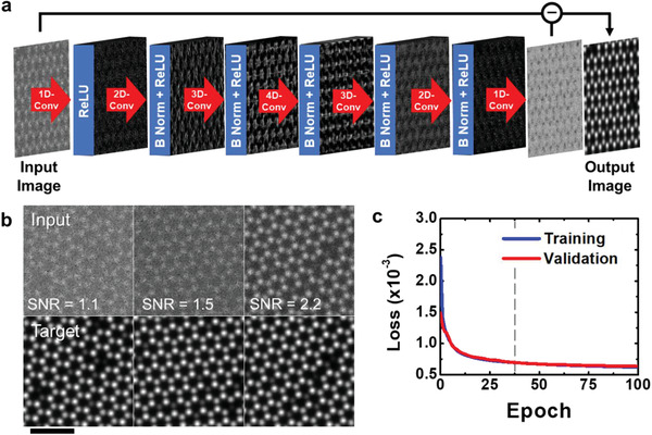
Figure 1
Deep learningu2010based denoiser algorithm. a) Deep neural network model constructed for denoising process for ADF STEM image of Vu2010WSe 2 . b) Examples of training dataset prepared for deep learnin...
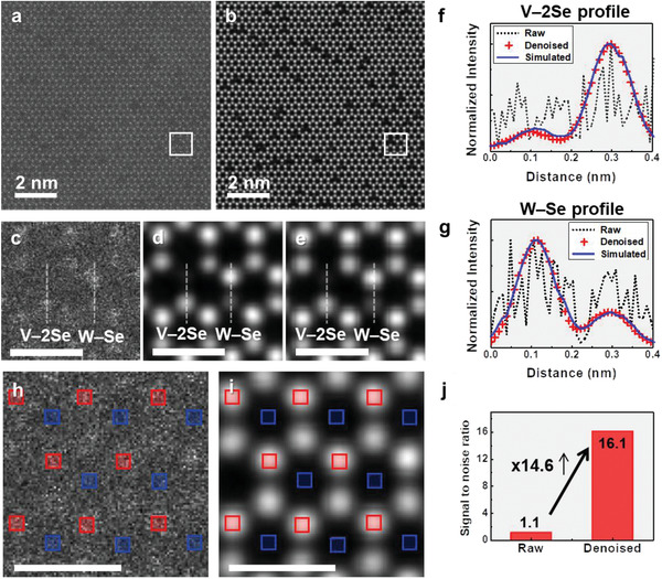
Figure 2
Restoration of noisy experimental ADFu2010STEM image of Vu2010doped WSe 2 by denoising process. a) A raw ADF STEM image recorded at high scanning rate of 1 u00b5s pix u22121 . b) Restored ADF STEM ima...
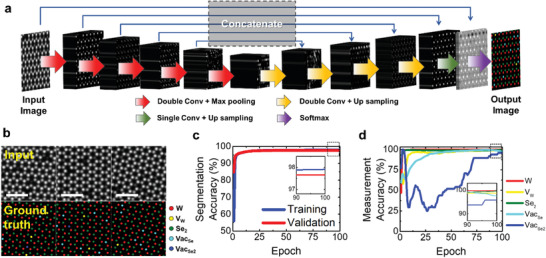
Figure 3
Deep learningu2010based algorithm for atomic site classification. a) Deep neural networks model constructed for quantification analysis of ADFu2010STEM image of Vu2010WSe 2 . b) Examples of training d...
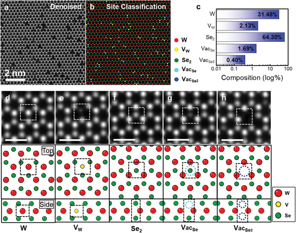
Figure 4
Automated quantification of dopants and defects in Vu2010WSe 2 monolayer. a) Denoised ADF STEM image of Vu2010WSe 2 . b) Deep learningu2010assisted atomic site mapping of Vu2010WSe 2 . c) Result of co...
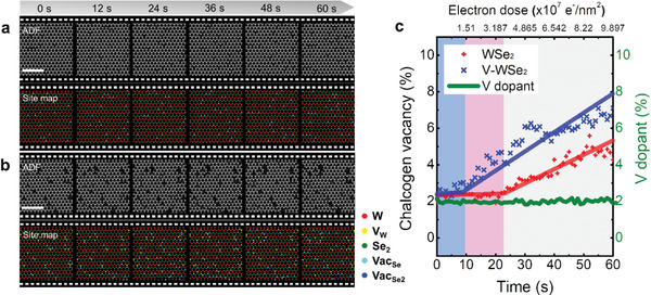
Figure 5
Application of the automated quantification algorithm to large imaging data volumes of (doped) WSe 2 showing dynamic defect evolutions under electron beam irradiation. a,b) (top) Series of ADF STEM im...
Figure images are served from the NIH/NLM PubMed Central Open Access Subset or Europe PMC; copyright remains with the publishers and authors.
💬 Discussion
0 commentsNo comments yet. Be the first to start a discussion!
Leave a Comment