Abstract
Exploring the maximum spatial resolution achievable in far-field optical imaging, we show that applying solid immersion lenses (SIL) in stimulated emission depletion (STED) microscopy addresses single spins with a resolution down to 2.4 ± 0.3 nm and with a localization precision of 0.09 nm.
🔬 Techniques
🧪 Sample Preparation
🏭 Microscope Brands
🏛️ Research Organizations (ROR)
Affiliated research institutions:
📋 Methods
STED-ODMR Setup : The components of the setup utilized for our experiments ( Figure 1 ) have been detailed elsewhere. 12 The NV centers in the diamond are excited by a triggerable diode laser (Pico TA, Picoquant, Berlin, Germany) operating at 532 nm and providing pulses of ∼100 ps duration. Stimulated emission is induced by a frequency-doubled fiber laser (IPG Photonics, Oxford, USA) emitting at 775 nm at a repetition rate of ∼8 MHz and a pulse length of 3 ns. The STED beam passes through an optical glass plate (RPC Photonics, Rochester, NY, USA) imposing a 0–2π helical phase-ramp which generates the desired toroidally (doughnut) shaped intensity distribution in the focal region. The two beams are spatially superimposed by dichroic mirrors and focused by the objective lens (100x oil immersion, NA = 1.4, Leica, Wetzlar, Germany). Fluorescence emitted from the sample is collected by the same objective lens and filtered to block STED and excitation light. The remaining fluorescence is focused onto the core of a multimode fiber which acts as confocal pinhole, and is finally detected by an avalanche photodiode (Perkin & Elmer, Waltham, USA). Scanning the sample directly yields the (subdiffraction resolution) image as raw data. SIL Production : The SILs were fabricated directly in the diamond by ablating the diamond with a focused beam of 30 keV gallium ions. 15 , 16 As the focal extent of the gallium beam is ≍10 nm in diameter, any residual surface roughness is much smaller than the wavelength range of the light involved (532–775 nm). We manufactured SILs ranging in size from 5–8 μm in diameter in two diamond samples. The first was a sample of high-purity polycrystalline diamond grown by chemical-vapor deposition. We directly milled several SILs of 5 μm diameter in this sample randomly placed on single crystallites. The density of single NVs in the sample is sufficiently high that a useful fraction of the SILs couple to individual or sparse ensembles of NV centers. One SIL in particular was found both to be coupled to a single defect center (as confirmed with single-photon antibunching measurements) and showed a 10-fold increase in detected fluorescence. The second sample was a high purity single crystal diamond in which regular arrays of NV centers had been generated at a depth of 4 μm by implantation of 6 MeV nitrogen ions followed by annealing at 800 °C. The 8 μm diameter SILs etched in this sample were registered to individual defects. Here, the best SIL showed an 8-fold increase in collected fluorescence. It is also worth noting that, while the SIL is small, the diamond-air interface for the SILs under investigation is 12–15 λ from the emitter and so the solid immersion provided by the SIL maintains far-field optical conditions.
Show full methods section
STED-ODMR Setup : The components of the setup utilized for our experiments ( Figure 1 ) have been detailed elsewhere. 12 The NV centers in the diamond are excited by a triggerable diode laser (Pico TA, Picoquant, Berlin, Germany) operating at 532 nm and providing pulses of ∼100 ps duration. Stimulated emission is induced by a frequency-doubled fiber laser (IPG Photonics, Oxford, USA) emitting at 775 nm at a repetition rate of ∼8 MHz and a pulse length of 3 ns. The STED beam passes through an optical glass plate (RPC Photonics, Rochester, NY, USA) imposing a 0–2π helical phase-ramp which generates the desired toroidally (doughnut) shaped intensity distribution in the focal region. The two beams are spatially superimposed by dichroic mirrors and focused by the objective lens (100x oil immersion, NA = 1.4, Leica, Wetzlar, Germany). Fluorescence emitted from the sample is collected by the same objective lens and filtered to block STED and excitation light. The remaining fluorescence is focused onto the core of a multimode fiber which acts as confocal pinhole, and is finally detected by an avalanche photodiode (Perkin & Elmer, Waltham, USA). Scanning the sample directly yields the (subdiffraction resolution) image as raw data. SIL Production : The SILs were fabricated directly in the diamond by ablating the diamond with a focused beam of 30 keV gallium ions. 15 , 16 As the focal extent of the gallium beam is ≍10 nm in diameter, any residual surface roughness is much smaller than the wavelength range of the light involved (532–775 nm). We manufactured SILs ranging in size from 5–8 μm in diameter in two diamond samples. The first was a sample of high-purity polycrystalline diamond grown by chemical-vapor deposition. We directly milled several SILs of 5 μm diameter in this sample randomly placed on single crystallites. The density of single NVs in the sample is sufficiently high that a useful fraction of the SILs couple to individual or sparse ensembles of NV centers. One SIL in particular was found both to be coupled to a single defect center (as confirmed with single-photon antibunching measurements) and showed a 10-fold increase in detected fluorescence. The second sample was a high purity single crystal diamond in which regular arrays of NV centers had been generated at a depth of 4 μm by implantation of 6 MeV nitrogen ions followed by annealing at 800 °C. The 8 μm diameter SILs etched in this sample were registered to individual defects. Here, the best SIL showed an 8-fold increase in collected fluorescence. It is also worth noting that, while the SIL is small, the diamond-air interface for the SILs under investigation is 12–15 λ from the emitter and so the solid immersion provided by the SIL maintains far-field optical conditions.
Supporting Information Supporting Information is available from the Wiley Online Library or from the author.
📊 Figures
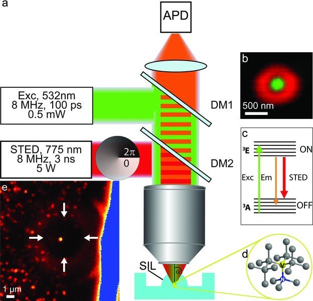
Figure 1
a) STED nanoscope for optical detection of magnetic resonances (ODMR), addressing individual diamond nitrogen vacancy (NV) centers inside a solid immersion lens (SIL) made of bulk diamond. STED nanosc...
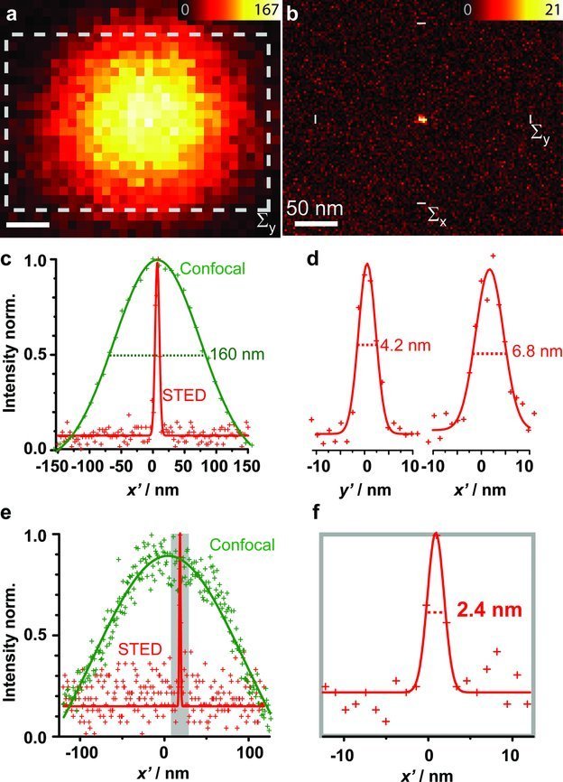
Figure 2
a) Confocal and b) STED image of a single NV located underneath a SIL yielding the effective point spread function (E-PSF) of the SIL-STED microscopy c) The SIL-enhanced confocal E-PSF has a FWHM of 1...
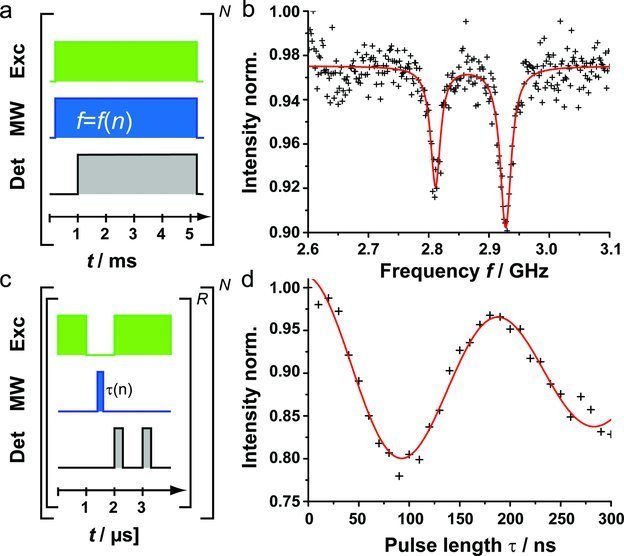
Figure 3
Optical detection of magnetic resonances of NV electron spins with SIL-STED. a) Sequence of optical excitation (Exc), microwave exposure (MW), and detection time window (Det) used for recording an b) ...
Figure images are served from the NIH/NLM PubMed Central Open Access Subset or Europe PMC; copyright remains with the publishers and authors.
💬 Discussion
0 commentsNo comments yet. Be the first to start a discussion!
Leave a Comment