Abstract
Cryo-electron tomography (cryoET) has become a powerful technique at the interface of structural biology and cell biology, due to its unique ability for imaging cells in their native state and determining structures of macromolecular complexes in their cellular context. A limitation of cryoET is its restriction to relatively thin samples. Sample thinning by cryo-focused ion beam (cryoFIB) milling has significantly expanded the range of samples that can be analyzed by cryoET. Unfortunately, cryoFIB milling is low-throughput, time-consuming and manual. Here, we report a method for fully automated sequential cryoFIB preparation of high-quality lamellae, including rough milling and polishing. We reproducibly applied this method to eukaryotic and bacterial model organisms, and show that the resulting lamellae are suitable for cryoET imaging and subtomogram averaging. Since our method reduces the time required for lamella preparation and minimizes the need for user input, we envision the technique will render previously inaccessible projects feasible.
🔬 Techniques
🧬 Organisms
💻 Software
🧪 Sample Preparation
🏭 Microscope Brands
🧪 Reagent Suppliers
📷 Detectors
💻 Software Details
💾 Data Repositories
🏛️ Research Organizations (ROR)
Affiliated research institutions:
📋 Methods
Overview of the equipment and workflow
The method was established and tested on two different Crossbeam 550 FIB-SEM instruments (Carl Zeiss Microscopy) equipped with copper band-cooled mechanical cryo-stages and integrated VCT500 vacuum transfer systems (Leica Microsystems). The detectors used included an InLens secondary electron detector for determining grid topology (Carl Zeiss Microscopy) and a SE2 detector for identifying milling targets and visually assessing the ice thickness (Carl Zeiss Microscopy). In our workflow, EM grids were prepared with the yeast strain Saccharomyces cerevisiae SK1 and the cyanobacterial strain Anabaena sp. PCC 7120, clipped into FIB milling Autogrids (ThermoFisher Scientific, Waltham, MA). These grids were then mounted onto a pre-tilted Autogrid holder ( Medeiros et al., 2018 ) (Leica Microsystems GmbH, Vienna, Austria) using a VCM loading station (Leica Microsystems). With the VCT500 shuttle, the Autogrid holder was transferred to an ACE600 cryo-sputter coater (Leica Microsystems). Under cryogenic conditions the plunge-frozen sample were sputter-coated with a ~4 nm thick layer of tungsten. After sputter coating, the samples were transferred into the Crossbeam 550 using the VCT500 shuttle. In the Crossbeam 550, the gas injection system (GIS) was used to deposit an organometallic platinum precursor layer onto each grid. Automated sequential FIB milling was subsequently set up and executed. Sample preparation, plunge-freezing, Autogrid mounting, holder loading and vacuum cryo-transfer steps were executed similarly to what was described in Medeiros et al. (2018) . Any deviations to the previously published protocol are described below.
Show full methods section
Overview of the equipment and workflow
The method was established and tested on two different Crossbeam 550 FIB-SEM instruments (Carl Zeiss Microscopy) equipped with copper band-cooled mechanical cryo-stages and integrated VCT500 vacuum transfer systems (Leica Microsystems). The detectors used included an InLens secondary electron detector for determining grid topology (Carl Zeiss Microscopy) and a SE2 detector for identifying milling targets and visually assessing the ice thickness (Carl Zeiss Microscopy). In our workflow, EM grids were prepared with the yeast strain Saccharomyces cerevisiae SK1 and the cyanobacterial strain Anabaena sp. PCC 7120, clipped into FIB milling Autogrids (ThermoFisher Scientific, Waltham, MA). These grids were then mounted onto a pre-tilted Autogrid holder ( Medeiros et al., 2018 ) (Leica Microsystems GmbH, Vienna, Austria) using a VCM loading station (Leica Microsystems). With the VCT500 shuttle, the Autogrid holder was transferred to an ACE600 cryo-sputter coater (Leica Microsystems). Under cryogenic conditions the plunge-frozen sample were sputter-coated with a ~4 nm thick layer of tungsten. After sputter coating, the samples were transferred into the Crossbeam 550 using the VCT500 shuttle. In the Crossbeam 550, the gas injection system (GIS) was used to deposit an organometallic platinum precursor layer onto each grid. Automated sequential FIB milling was subsequently set up and executed. Sample preparation, plunge-freezing, Autogrid mounting, holder loading and vacuum cryo-transfer steps were executed similarly to what was described in Medeiros et al. (2018) . Any deviations to the previously published protocol are described below.
Cell culture and plunge freezing
FIB milling tests were performed using the cyanobacterial strain Anabaena sp. PCC 7120 and the yeast strain Saccharomyces cerevisiae SK1 ( Table 2 ). Yeast and cyanobacterial strain identities were determined according to standard microbiological procedures. The cyanobacterial cell line originates from Rippka et al. (1979) . The cyanobacterial strain was grown and prepared for FIB milling as previously described in Weiss et al. (2019) . The yeast strain was generated in this study. Meiotic yeast cells were cultured as previously described in Wild et al. (2019) and prepared for plunge freezing as described by Medeiros et al. (2018) , with minor modifications. Briefly, yeast cells were harvested and 4 µL of cell suspension, OD 600 ∼1.5, was applied on glow-discharged copper EM grids (R2/2, Quantifoil, Großlöbichau, Germany). Grids were back-blotted twice for 3–5 s each time, at 4°C with 95% humidity and plunged into liquid ethane/propane using a Vitrobot (ThermoFisher). Table 2. Strains used in this work.
Strain Identifier Genotype Source or reference
Anabaena sp. PCC7120 Cyanobacteria Wild Type Rippka et al. (1979) Saccharomyces cerevisiae SK1 Yeast diploid, homozygous for ndt80∆::HIS3 ho::LYS2 ura3 leu2::hisG trp1::hisG his3::hisG This study Equipment calibration To ensure that automated sequential FIB milling was successful, the Crossbeam 550 was properly aligned. While the SEM column alignments are stable and non-essential during automated milling, the FIB alignment between different currents at a given voltage (30 kV for biological cryo-samples) should be checked and optimized. Typically, this calibration is done weekly or when deemed necessary and takes roughly 60 min to complete. In case of deviation, on-the-fly adjustments are possible on a loaded cryo-sample, however, standard calibration procedures are best performed on a silicon wafer due to its structural homogeneity, which allows better evaluation of the FIB beam shape. Once inserted into the chamber, the stage was tilted by 54° to be perpendicular to the FIB beam and then moved to the working distance (i.e. coincidence point). Using the ‘spot’ function in an unexposed sample region, the beam was focused to its spot size allowing it to burn a hole into the silicon. When the current is properly calibrated, the beam will produce a spot that is round with sharp edges. This was best seen when using a mixed signal of the InLens and SE2 detector. If a beam spot had imperfections, like a tailing edge, beam parameters including focus, stigmatism and aperture alignments need to be improved and saved. After optimizing these parameters for each current, all currents were aligned against the reference current. This was best performed by positioning an easily recognizable structure, like a burnt hole, in the middle of the reference current image and then centering this feature in each of the other currents. Finally, to ensure that the currents were properly aligned, a location is imaged by each current. If properly aligned, switching between currents should not lead to focus changes or beam offsets. Sample coating To enhance conductivity and decrease the effects of charging, the plunge-frozen sample was coated with a ~4 nm layer of tungsten. This was autonomously executed by an ACE600 sputter coating program in an argon atmosphere (8.0E-3 mbar) and with a current of 90 mA. After inserting the holder into the FIB-SEM, a protection layer of organometallic platinum precursor was deposited onto each grid to minimize the effects of curtaining. For cold deposition of platinum precursor, the holder was moved 3 mm below the coincidence point and tilted to 20°. By positioning the GIS needle above each grid and opening the GIS for 45 s, a layer of platinum precursor was deposited onto the sample. Since the GIS needle was mounted at a similar angle as the FIB column, deposition of platinum occurred preferentially on the side of the cells where the FIB beam hits the sample, ensuring the best protection. For deposition under cryo-conditions, it is essential that the heating element of the GIS needle and reservoir are turned off to keep the system at room temperature (28°C).
Stage registration
To assist in the identification of targets, overview images of an entire EM grid are taken. On the Zeiss Crossbeam 550, these images can be coupled to the stage navigation. To calibrate stage registration a high-resolution (4096 × 3072 pixels, 35x magnification) overview image was taken with the SE2 detector, which provided the best information for identifying targets inside the vitrified ice and determining ice thickness. This overview image was then loaded onto the stage navigation bar and registered by correlating three distinctive points on the image to their specific positions on the stage as observed in the live SEM view. After completion, double clicking on a desired target in the navigation bar automatically moves the stage to the location of interest. In addition, backlash correction was also included for all automated stage movements, using the user preference settings of the software SmartSEM (Carl Zeiss Microscopy). Defining milling materials To permit unsupervised automation of lamellae production, the Crossbeam 550 was calibrated to mill a cross-section with a specified depth through the sample. To ensure proper milling, the system needs to be calibrated for a distinct ‘material’ so that the correct milling parameters like dose are applied during milling. For cryo-TEM lamella preparation, the material ‘vitrified ice’ was created using a dose calibration of 20 mC/cm² being equivalent to a milling depth of 1 µm in cross-section mode. No attempts were made to make sample specific material types, however, this would also be possible. Parameters for imaging and milling For SEM imaging, voltages from 1.9 to 5 kV and a constant current of 28 pA were used. To capture SEM images, we most commonly used the InLens detector to obtain surface information of the sample. During FIB imaging, on the other hand, a fixed voltage of 30 kV and a low current (20 pA) was used. FIB images were usually captured by using the SE2 detector, which is less sensitive to imaging-induced charging. During automated sequential milling a total of four currents were used for rough milling (700 pA, 300 pA and 100 pA) and polishing (50 pA). For milling, we defined the patterns to be executed using bi-directional and cross-section cycle mode with a 10 µm milling depth. It is important to note that the milling parameters (milling current, pattern size, milling depth, etc.) are adjustable on-the-fly to optimize each set of patterns for the target location and desired milling strategy.
Automated sequential FIB milling protocol
To generate high-quality lamellae, it was essential to prepare the FIB-SEM and sample for automated sequential milling. Preparations included checking and calibrating the FIB currents, coating the plunge-frozen sample with a layer of tungsten and organometallic platinum, and performing stage registration. Once these steps were executed, automated sequential milling was initiated by identifying and setting up milling targets. The grid overview image in the stage navigator was used to identify a milling target. The identified target was then manually centered in the live FIB view with the aid of the SEM. To improve the accuracy of automated stage movements, backlash correction was performed manually and implemented for all automated stage movements. The target’s stage coordinates were then saved in the stage navigator. To ensure that the instrument was able to perform targeting during automation, the stage was manually moved away from the target and then instructed to move back to its saved location. The target was located using the live FIB view and if it was >1 µm from desired location, it was manually centered again. If manual centering was required, the new stage location was saved and the instrument’s ability to perform targeting was tested again. To ensure successful milling during automation, it was essential to refine the stage location until the stage was able to perform targeting successfully. Once an accurate stage movement was achieved, milling patterns were placed onto a targets FIB image captured using SmartFIB. In SmartFIB, each pattern contains specific milling conditions (i.e. current, milling depth, size, shape, etc.) and a designated FIB milling location. SmartFIB allows the placing of multiple patterns with different conditions onto a single FIB image in order to perform automated milling. Patterns were placed and their properties were changed by using the SmartFIB GUI in the ‘attributes’ tab. When testing this methodology, we placed eight rectangular milling patterns: six rough milling and two polishing patterns ( Table 3 ). The final polishing patterns were spaced 300 nm apart, since we generally expected the generated lamellae to be thinner than the specified value. To make uniform lamellae, it was also possible to save these eight patterns as a recipe, which can be dragged and dropped onto images of other milling targets. To then save these milling patterns, it was essential to separate the rough and polishing patterns. This was accomplished by deleting the polishing patterns from our recipe, saving only the rough milling patterns, undoing the deletion of the polishing patterns (using the SmartFIB ‘undo’ button), deleting all rough milling patterns and then saving only the polishing patterns. Table 3. Dimensions and currents used for each milling pattern during automated sequential lamellae preparation. Milling Pattern # Pattern Attributes Milling pattern 1 and 2 (Rough Milling 1) 30 kV 700 pA 9 × 5 µm rectangle Generates 2 µm thick lamella Milling Pattern 3 and 4 (Rough Milling 2) 30 kV 300 pA 8 × 2 µm rectangle Generates 1 µm thick lamella Milling Pattern 5 and 6 (Rough Milling 3) 30 kV 100 pA 7.5 × 1 µm rectangle Generates 500 nm thick lamella Milling Pattern 7 and 8 (Lamella Polishing) 30 kV 50 pA 7 × 0.5 µm rectangle Generates 300 nm thick lamella Drift Correction Pattern (Rough Milling and Polishing) 3 × 3 µm rectangle To improve the targeting accuracy of this methodology, a drift correction step was also added to each set of rough milling and polishing patterns immediately before being saved. This was done in the SmartFIB ‘attributes’ tab, by capturing and saving an image of a defined region of the FIB view.
During the automated protocol
SmartFIB would use this image to perform image recognition before beginning milling and compensate for small shifts (generally between 0 and 2 µm) to ensure the milling patterns are placed correctly on the target. When testing this methodology, it was important to use the same drift correction image for both the rough milling and polishing patterns. This ensured that the same region is exposed during rough milling and polishing. After saving a set of rough and polishing patterns, the described method can be repeated for further targets. For an automated protocol, about 9 min were needed to set up each target. Once satisfied with the number of targets, all rough milling recipes in the SmartFIB queue were selected and exposed. Exposure of a typical rough milling target took about 12 min. Upon completion, rough milling targets were observed using the SEM and FIB to determine their quality. To then initiate polishing, it is possible to either tick all polishing recipes and expose them, or individually move to each target using SmartFIB, take a FIB image, manually drag polishing patterns into place and expose the lamella. Polishing typically took about 4.75 min. Once all targets are polished, the lamellae are removed from the instrument and stored. Note that instrument 2 ( Table 1 ) suffered from stage drift, which caused issues during polishing. Unfortunately, SmartFIB does not have an integrated wait time, however, using a set of low current (1–5 pA) patterns, we were able to apply a wait time of 3 min to allow the stage to settle before polishing. An overview of all the milling attempts that were performed can be found in Table 1 . Cryo-electron tomography, tomogram reconstruction and subtomogram averaging Data was collected on a Titan Krios 300kV electron microscope (ThermoFisher) equipped with a field emission gun, imaging filter (Gatan, Pleasanton, U.S.) (slit width 20 eV) and K2 or K3 direct electron detector (Gatan). To generate an overview of each grid, grid montages were collected at 135x magnification using SerialEM ( Mastronarde, 2005 ). Cyanobacteria data was collected with UCSF Tomo ( Zheng et al., 2007 ) at 2° increments between +60° and −60°. Data was collected at a defocus of −8 µm, total accumulated dose of ~140 e - / Å 2 and pixel size of 3.38 Å. Yeast tomograms were collected using SerialEM between +60° and −60° at 2° increments with a defocus of −8 µm, total accumulated dose of ~120 e - / Å 2 and pixel size of 4.57 Å. Tomogram reconstruction and subtomogram averaging was performed according to Weiss et al. (2019) . Briefly, tomograms were reconstructed using the IMOD package ( Kremer et al., 1996 ) and septal junction subtomogram averaging was performed using PEET ( Nicastro et al., 2006 ). A total of 412 particles were extracted and averaged in a box of 44 × 44 × 44 pixels with a pixel size of 6.8 Å. PEET classification was then used to remove misaligned particles (343 final particles). 5-fold symmetry was applied to obtain the final average. The FSC (Fourier Shell Correlation) was generated by using the PEET command calcFSC.
Defining milling materials To permit unsupervised automation of lamellae production, the Crossbeam 550 was calibrated to mill a cross-section with a specified depth through the sample. To ensure proper milling, the system needs to be calibrated for a distinct ‘material’ so that the correct milling parameters like dose are applied during milling. For cryo-TEM lamella preparation, the material ‘vitrified ice’ was created using a dose calibration of 20 mC/cm² being equivalent to a milling depth of 1 µm in cross-section mode. No attempts were made to make sample specific material types, however, this would also be possible.
Automated sequential FIB milling protocol
To generate high-quality lamellae, it was essential to prepare the FIB-SEM and sample for automated sequential milling. Preparations included checking and calibrating the FIB currents, coating the plunge-frozen sample with a layer of tungsten and organometallic platinum, and performing stage registration. Once these steps were executed, automated sequential milling was initiated by identifying and setting up milling targets. The grid overview image in the stage navigator was used to identify a milling target. The identified target was then manually centered in the live FIB view with the aid of the SEM. To improve the accuracy of automated stage movements, backlash correction was performed manually and implemented for all automated stage movements. The target’s stage coordinates were then saved in the stage navigator. To ensure that the instrument was able to perform targeting during automation, the stage was manually moved away from the target and then instructed to move back to its saved location. The target was located using the live FIB view and if it was >1 µm from desired location, it was manually centered again. If manual centering was required, the new stage location was saved and the instrument’s ability to perform targeting was tested again. To ensure successful milling during automation, it was essential to refine the stage location until the stage was able to perform targeting successfully. Once an accurate stage movement was achieved, milling patterns were placed onto a targets FIB image captured using SmartFIB. In SmartFIB, each pattern contains specific milling conditions (i.e. current, milling depth, size, shape, etc.) and a designated FIB milling location. SmartFIB allows the placing of multiple patterns with different conditions onto a single FIB image in order to perform automated milling. Patterns were placed and their properties were changed by using the SmartFIB GUI in the ‘attributes’ tab. When testing this methodology, we placed eight rectangular milling patterns: six rough milling and two polishing patterns ( Table 3 ). The final polishing patterns were spaced 300 nm apart, since we generally expected the generated lamellae to be thinner than the specified value. To make uniform lamellae, it was also possible to save these eight patterns as a recipe, which can be dragged and dropped onto images of other milling targets. To then save these milling patterns, it was essential to separate the rough and polishing patterns. This was accomplished by deleting the polishing patterns from our recipe, saving only the rough milling patterns, undoing the deletion of the polishing patterns (using the SmartFIB ‘undo’ button), deleting all rough milling patterns and then saving only the polishing patterns. Table 3. Dimensions and currents used for each milling pattern during automated sequential lamellae preparation. Milling Pattern # Pattern Attributes Milling pattern 1 and 2 (Rough Milling 1) 30 kV 700 pA 9 × 5 µm rectangle Generates 2 µm thick lamella Milling Pattern 3 and 4 (Rough Milling 2) 30 kV 300 pA 8 × 2 µm rectangle Generates 1 µm thick lamella Milling Pattern 5 and 6 (Rough Milling 3) 30 kV 100 pA 7.5 × 1 µm rectangle Generates 500 nm thick lamella Milling Pattern 7 and 8 (Lamella Polishing) 30 kV 50 pA 7 × 0.5 µm rectangle Generates 300 nm thick lamella Drift Correction Pattern (Rough Milling and Polishing) 3 × 3 µm rectangle To improve the targeting accuracy of this methodology, a drift correction step was also added to each set of rough milling and polishing patterns immediately before being saved. This was done in the SmartFIB ‘attributes’ tab, by capturing and saving an image of a defined region of the FIB view.
During the automated protocol
SmartFIB would use this image to perform image recognition before beginning milling and compensate for small shifts (generally between 0 and 2 µm) to ensure the milling patterns are placed correctly on the target. When testing this methodology, it was important to use the same drift correction image for both the rough milling and polishing patterns. This ensured that the same region is exposed during rough milling and polishing. After saving a set of rough and polishing patterns, the described method can be repeated for further targets. For an automated protocol, about 9 min were needed to set up each target. Once satisfied with the number of targets, all rough milling recipes in the SmartFIB queue were selected and exposed. Exposure of a typical rough milling target took about 12 min. Upon completion, rough milling targets were observed using the SEM and FIB to determine their quality. To then initiate polishing, it is possible to either tick all polishing recipes and expose them, or individually move to each target using SmartFIB, take a FIB image, manually drag polishing patterns into place and expose the lamella. Polishing typically took about 4.75 min. Once all targets are polished, the lamellae are removed from the instrument and stored. Note that instrument 2 ( Table 1 ) suffered from stage drift, which caused issues during polishing. Unfortunately, SmartFIB does not have an integrated wait time, however, using a set of low current (1–5 pA) patterns, we were able to apply a wait time of 3 min to allow the stage to settle before polishing. An overview of all the milling attempts that were performed can be found in Table 1 .
Additional files Transparent reporting form
📊 Figures

Figure 1.
Schematic of the automated sequential cryoFIB milling workflow.
( A ) FIB currents are aligned and calibrated, and the sample is loaded into the FIB-SEM instrument. ( B ) A target cell is identified on the grid with the SEM andu00a0FIB. ( C ) To correct for errors...

Figure 1u2014figure supplement 1.
Schematic of the manual cryoFIB milling workflow.
( A ) The sample is loaded into the FIB-SEM instrument. ( B ) A target is centered in the FIB image. ( Cu2013E ) The first pair of rough milling patterns is placed on the target and milling is execute...
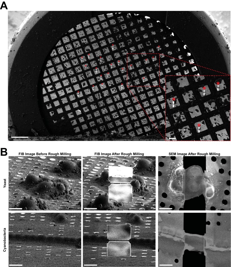
Figure 2.
Representative images of lamellae generated by automated sequential rough milling.
( A ) SEM grid overview image including 20 yeast targets (asterisks) on which rough milling was performed in an automated sequential manner (session C). Bars, 200 u00b5m. ( B ) Representative SEM and ...

Figure 2u2014figure supplement 1.
Further examples of lamellae generated in a fully automated manner.
Images of lamellae from yeast cells at three different stages of the workflow. The left column shows SEM images of five polished lamellae ( Au2013E ). The middle column shows TEM images of the same la...

Figure 2u2014figure supplement 2.
Distribution of lamellae thicknesses.
The plot shows the distribution of the thickness values of fully automated sequential FIB-milled lamellae, as determined by cryoET imaging. The final polishing milling patterns were spaced 300 nm apar...

Figure 3.
Automated sequential cryoFIB milling results in high-quality lamellae and cryotomograms.
( A ) CryoTEM overview image of a lamella (session H) containing three yeast cells. Red mark indicates the area imaged in ( B ). Bar, 5 u00b5m. ( B ) A 22.85 nm thick slice through a cryo-tomogram of ...

Figure 3u2014figure supplement 1.
Comparison of data quality between manual and automated milling.
Shown is a Fourier Shell Correlation (FSC) curve (red) for the septal junction subtomogram average shown in Figure 3F (resulting from automated milling). The second curve (blue) results from a dataset...
Figure images are served from the NIH/NLM PubMed Central Open Access Subset or Europe PMC; copyright remains with the publishers and authors.
💬 Discussion
0 commentsNo comments yet. Be the first to start a discussion!
Leave a Comment